Semiconductor device and method of manufacturing the same

a semiconductor and manufacturing method technology, applied in the direction of printed circuit aspects, coatings, and metal adhesion improvement of the insulation substrate, can solve the problems of unlikely tilting or dislodging of the projected electrode, and achieve the effects of high reliability, enhanced joint reliability of a semiconductor apparatus with a three-dimensional mounting structure, and convenient configuration

Active Publication Date: 2009-06-11
PANASONIC SEMICON SOLUTIONS CO LTD
View PDF14 Cites 113 Cited by
  • Summary
  • Abstract
  • Description
  • Claims
  • Application Information

AI Technical Summary

Benefits of technology

[0014]According to the configuration described above, the protruding portion of the projected electrode protrudes from the front face of the molding resin portion and the distal end of the protruding portion is a flat face. Therefore, when configuring a semiconductor apparatus with a three-dimensional mounting structure such as a PoP semiconductor apparatus, by using the present semiconductor device as a lower-level semiconductor device, a rear-face projected electrode of another semiconductor device stacked on an upper level can be stably joined to the distal end face of the projected electrode of the lower-level semiconductor device. In other words, when mounting a semiconductor device whose rear-face projected electrode has a spherically-shaped distal end such as a BGA (Ball Grid Array) semiconductor device, since the distal end face of a projected electrode of a lower-level semiconductor device is flat, an upper-level semiconductor device is not horizontally displaced and variations in horizontal mounting positions of the upper-level semiconductor device can be suppressed even when the pressing force during mounting presses the rear-face projected electrode in a vertical direction against the distal end face of the projected electrode of the lower-level semiconductor device. Therefore, a semiconductor apparatus with a highly reliable three-dimensional mounting structure can be realized.
[0037]According to the present invention, the joint reliability of a semiconductor apparatus with a three-dimensional mounting structure can be enhanced, and a PoP semiconductor apparatus can be readily configured with high reliability and at low cost. As such, the present invention is useful in various electronic devices and, in particular, in mobile electronic devices.

Problems solved by technology

Furthermore, tilting or dislodging of the projected electrode is unlikely to occur between fixing of the projected electrode to the substrate and performing molding with resin.

Method used


Image

  • Semiconductor device and method of manufacturing the same
  • Semiconductor device and method of manufacturing the same
  • Semiconductor device and method of manufacturing the same

Examples


first embodiment

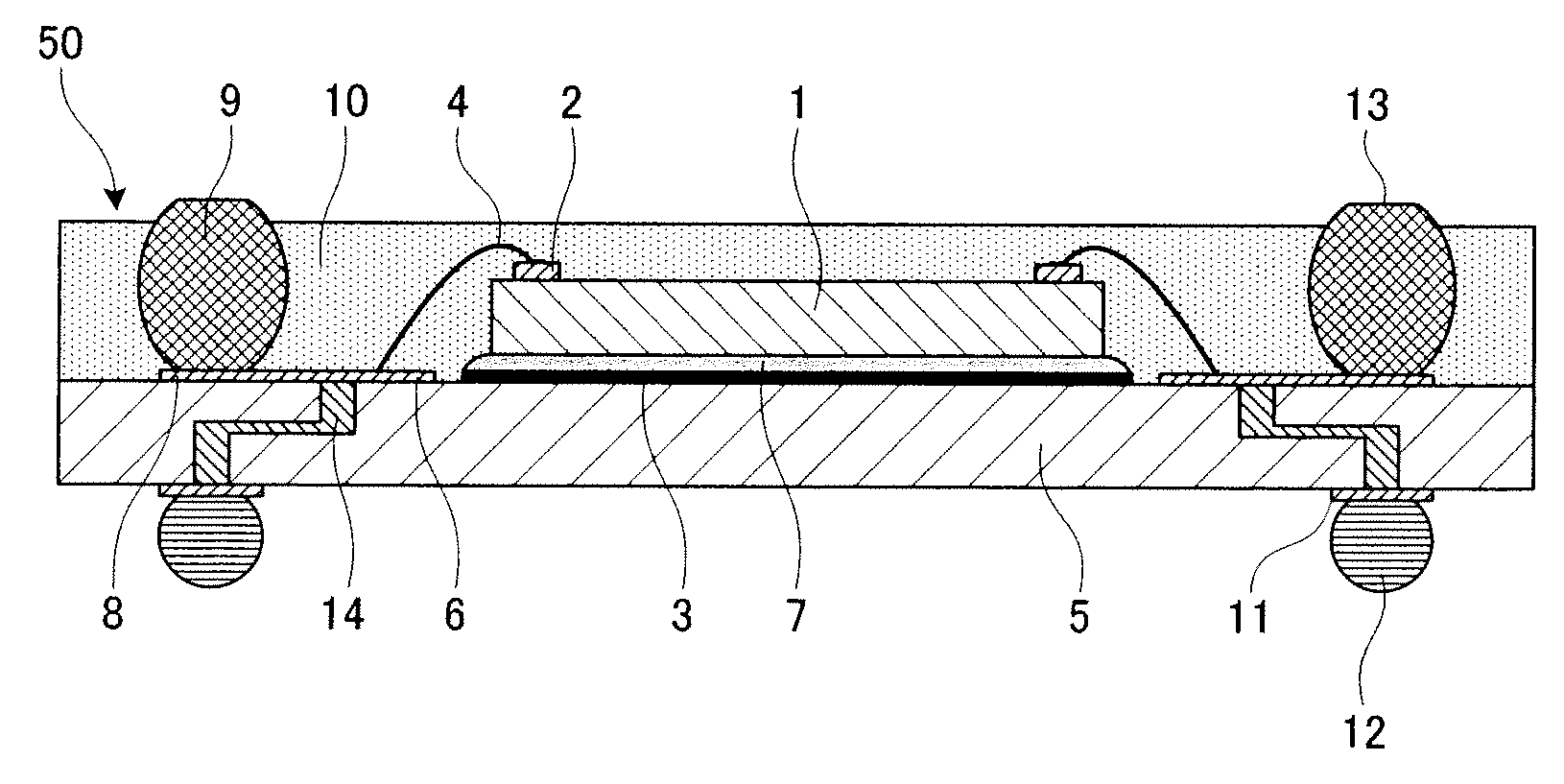
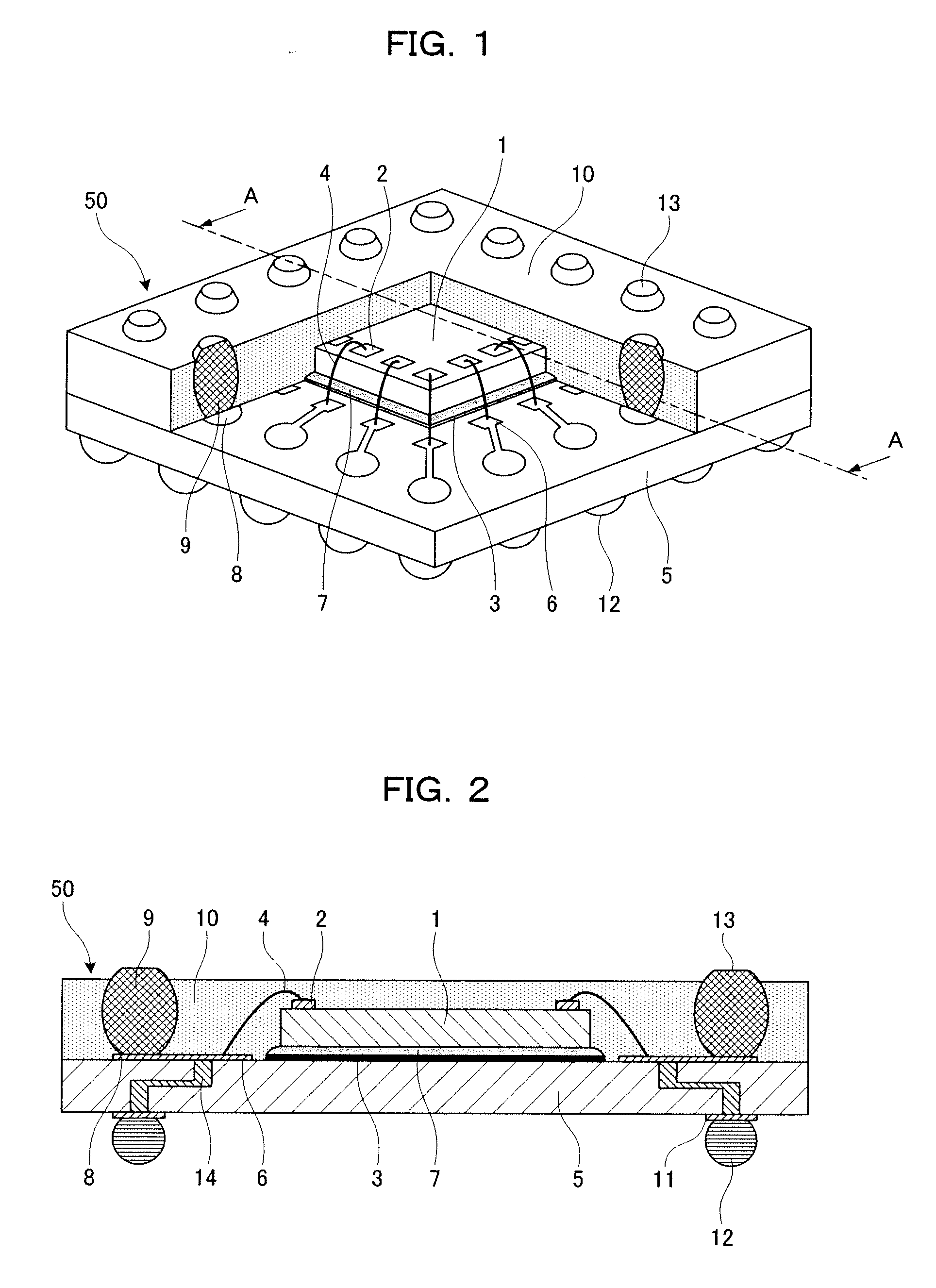
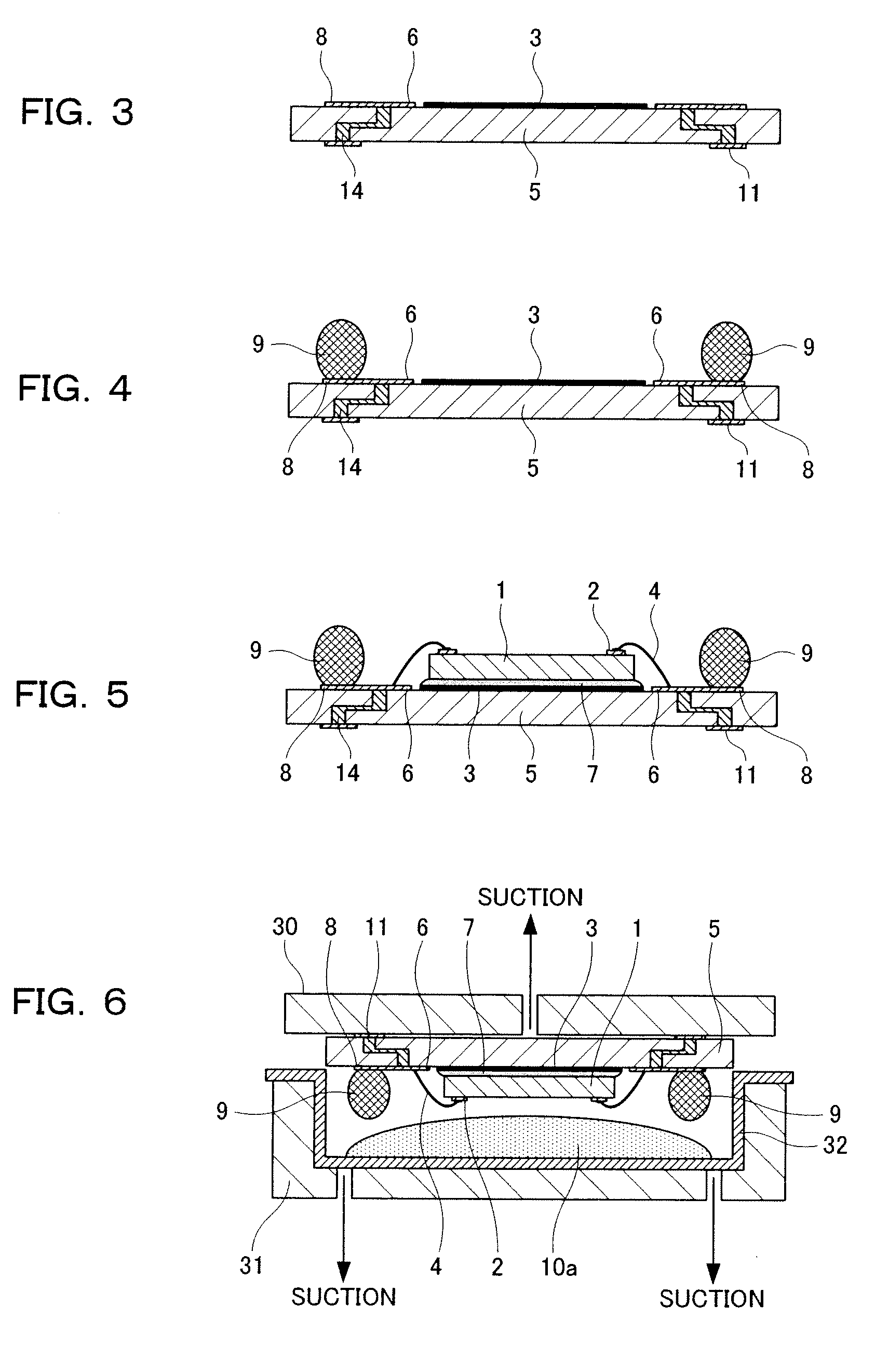
[0071]FIG. 1 is a perspective view showing a partially cutaway semiconductor device according to a first embodiment of the present invention, and FIG. 2 is a cross-sectional view of the semiconductor device taken along line A-A in FIG. 1.

[0072]In FIGS. 1 and 2, a semiconductor device 50 includes: a substrate 5; a semiconductor element 1 mounted in an element mounting region on one face (a front face) of the substrate 5 and electrically connected to the substrate 5 via a thin metallic wire 4; and a molding resin portion 10 formed on the front face of the substrate 5 so as to embed the semiconductor element 1 and the thin metallic wire 4.

[0073]The substrate 5 includes: a die pattern 3 and a plurality of connecting terminals 6 in the element mounting region on the front face; a plurality of laminated lands 8, respectively connected to the plurality of connecting terminals 6, in a region outside of the element mounting region; and a plurality of rear-face lands 11, respectively connecte...

second embodiment

[0111]FIG. 13 is a cross-sectional view showing the configuration of a semiconductor device according to a second embodiment of the present invention. The same members as the members described earlier in the first embodiment are assigned the same reference characters and descriptions thereof will be omitted. Thus, only points that differ from the semiconductor devices according to the above-described first embodiment shall be described. In a semiconductor device 51 according to the present second embodiment, a semiconductor element 17 is mounted on a substrate 15 using a flip-chip method. A plurality of bumps 18 connected to an internal circuit is formed at predetermined positions on the principal face of the semiconductor element 17. Semiconductor element lands 16 are formed in the center of the front face of the substrate 15 in an arrangement corresponding to the bumps 18 of the semiconductor element 17. The substrate 15 does not have the die patterns and connecting terminals desc...

third embodiment

[0114]FIG. 14 is a cross-sectional view showing the configuration of a semiconductor device according to a third embodiment of the present invention. The same members as the members described earlier in the first and second embodiments are assigned the same reference characters and descriptions thereof will be omitted. Thus, only points that differ from the semiconductor devices according to the above-described first and second embodiments shall be described. In a semiconductor device 52 according to the present third embodiment, a semiconductor element 19 and a semiconductor element 21 are laminated. The semiconductor element 19 adhered onto a die pattern 3 includes a plurality of connecting terminals 20 formed at the center of the principal front face thereof, and the semiconductor element 21 whose projected area is smaller than the semiconductor element 19 is connected on top of the semiconductor element 19 via bumps 22 using a flip-chip method.

[0115]The bumps 22 may be either bu...


PUM

PropertyMeasurementUnit
thicknessaaaaaaaaaa
thicknessaaaaaaaaaa
heightaaaaaaaaaa

Abstract

A semiconductor device capable of realizing highly reliable three-dimensional mounting, and a method of manufacturing the same, are provided. A projected electrode 9 is formed in a region outside of an element mounting region of a substrate 5. The projected electrode 9 includes a protruding portion that protrudes from the front face of a molding resin portion 10. The distal end of the protruding portion is a flat face 13. In addition, a portion of the projected electrode 9 whose cross section is larger than the protruding portion is positioned inside the molding resin portion 10.

Description

FIELD OF THE INVENTION[0001]The present invention relates to a semiconductor device to be used in a semiconductor apparatus with a three-dimensional mounting structure, and a method of manufacturing the semiconductor device.BACKGROUND OF THE INVENTION[0002]In recent years, Package-on-Package (hereinafter referred to as “PoP”) semiconductor apparatuses have been used in mobile phones, digital cameras, mobile personal computers, and the like. As a semiconductor device to be used in a semiconductor apparatus with a three-dimensional mounting structure such as a PoP semiconductor apparatus, various low-profile / small-sized semiconductor devices that allow other semiconductor devices to be stacked on top are being proposed.[0003]A conventional semiconductor device enabling another semiconductor device to be stacked on top includes: a substrate; a semiconductor element mounted on one face (hereinafter referred to as a “front face” or a “substrate front face”) of the substrate; a molding re...

Claims


Application Information

Patent Timeline
Patent Type & Authority Applications(United States)
IPC IPC(8): H01L23/482H01L23/488H01L21/44
CPCB29C43/18B29C45/02B29C45/14655H01L21/565H01L23/3128H01L24/16H01L24/27H01L24/28H01L24/45H01L24/48H01L24/743H01L24/83H01L24/85H01L25/105H01L2224/16145H01L2224/16225H01L2224/16227H01L2224/29144H01L2224/2919H01L2224/29339H01L2224/32225H01L2224/32506H01L2224/45015H01L2224/45124H01L2224/45139H01L2224/45144H01L2224/45147H01L2224/4809H01L2224/48091H01L2224/48227H01L2224/49171H01L2224/73265H01L2224/743H01L2224/83101H01L2224/83192H01L2224/83856H01L2224/92247H01L2924/01013H01L2924/01014H01L2924/01025H01L2924/01029H01L2924/0103H01L2924/01038H01L2924/01046H01L2924/01047H01L2924/0105H01L2924/01073H01L2924/01078H01L2924/01079H01L2924/01082H01L2924/07802H01L2924/15173H01L2924/15174H01L2924/15192H01L2924/15311H01L2924/1532H01L2924/15331H01L2924/20751H01L2924/20752H01L2924/20753H05K3/3457H05K3/38H05K2201/0379H05K2201/10515H05K2201/10977H05K2203/0278H01L2924/0132H01L24/29H01L2224/83805H01L2924/01033H01L2924/01042H01L2924/01074H01L2924/01322H01L2924/014H01L2924/0665H01L24/05H01L2924/0133H01L2924/1815H01L2924/0134H01L2224/29109H01L2224/29111H01L2224/85H01L2924/3511H01L2924/1517H01L2225/1023H01L2225/1058H01L2224/291H01L2224/2929H01L2924/01028H01L2224/16235H01L2924/00014H01L2924/07025H01L2924/0635H01L2924/00H01L2924/01083H01L2924/01049H01L2924/00012H01L2924/0695H01L2924/15787H01L2924/181H01L2924/12042H01L24/73H01L2224/05554H01L24/49
Inventor SHIMIZU, YOSHIAKIYAMADA, YUICHIROFUKUDA, TOSHIYUKI
Owner PANASONIC SEMICON SOLUTIONS CO LTD
Why Eureka
Try Eureka