Control circuit for adjusting leading edge blanking time and power converting system using the same control circuit
a control circuit and control circuit technology, applied in the direction of power conversion systems, dc-dc conversion, instruments, etc., can solve the problems of high switching loss, poor power-saving capability of the system, and possible fault triggers in the over-current protection mechanism of the pwm control chip b>100/b>
- Summary
- Abstract
- Description
- Claims
- Application Information
AI Technical Summary
Benefits of technology
Problems solved by technology
Method used
Image

Examples
first embodiment
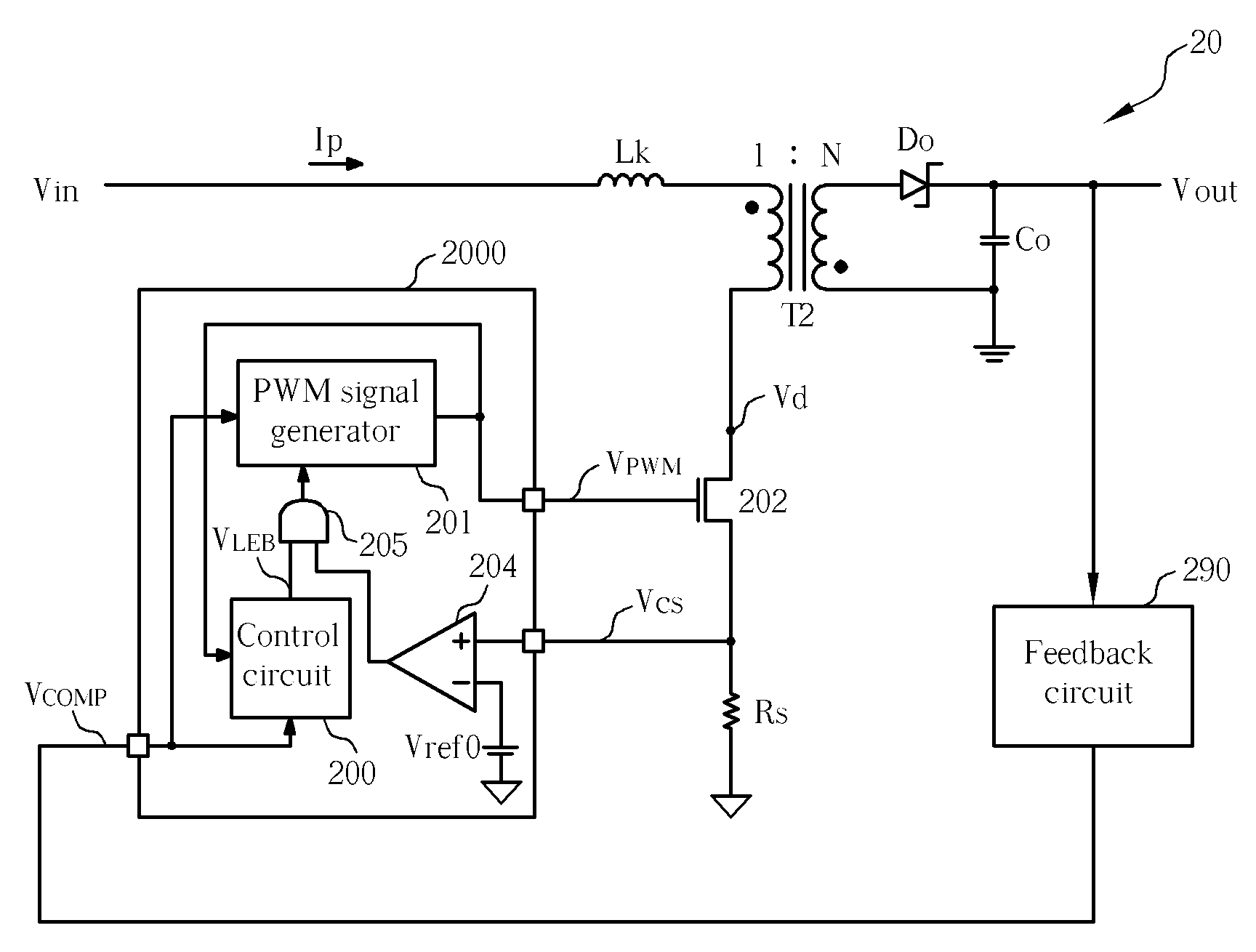
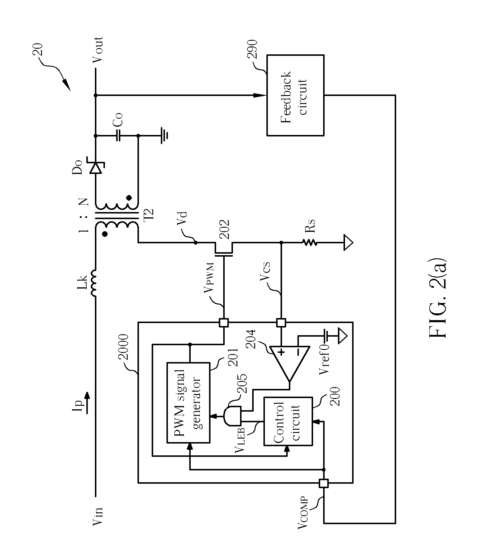
[0023]FIG. 2(b) is a diagram showing the control circuit 200 for adjusting a leading edge blanking time according to the present invention. The control circuit 200 includes a voltage-to-current converting circuit 210, a current mirror 220, a capacitor 232, a charge / discharge switch 234, a first comparator 240, a second comparator 250, a first current source 260, and a second current source 270.
[0024]The voltage-to-current converting circuit 210 generates a first current IR1 proportional to the voltage value of the feedback signal VCOMP (IR1=VCOMP / R1). The current mirror 220 generates a second current la identical to the first current IR1. The voltage-to-current converting circuit 210 and the current mirror 220 constitute a variable charging current generating circuit.
[0025]When the power switch 202 is turned on (i.e., the PWM signal VPWM is at logic high voltage), the charge / discharge switch 234 (an NMOS transistor) is turned off. A charging current IC1 charges the capacitor 232, wh...
second embodiment
[0032]In the second embodiment, the reference voltage Vref3 is used as the second threshold value Vth2 and the reference voltage Vref2 is used as the first threshold value Vth1. When the voltage value of the feedback signal VCOMP is between the reference voltage Vref2 and the reference voltage Vref3 (Vth1COMP2), both the second comparator 250 and the third comparator 350 output a logic high signal to turn on the transistors Q1 and Q4 and to turn off the transistors Q2 and Q5. The charging current IC1 is provided by the second current Ia, and the current value of the second current Ia is equal to the current value of the first current IR1, both are VCOMP / R1. Therefore, when the voltage value of the feedback signal VCOMP becomes larger, the charging current IC1 becomes larger and the leading edge blanking time TLEB becomes shorter. That is to say, the leading edge blanking time TLEB and the voltage value of the feedback signal VCOMP are inversely proportional.
[0033]When the voltage va...
PUM
 Abstract
Description
Claims
Application Information
 - R&D
- Intellectual Property
- Life Sciences
- Materials
- Tech Scout
- Unparalleled Data Quality
- Higher Quality Content
- 60% Fewer Hallucinations
Browse by: Latest US Patents, China's latest patents, Technical Efficacy Thesaurus, Application Domain, Technology Topic, Popular Technical Reports.
© 2025 PatSnap. All rights reserved.Legal|Privacy policy|Modern Slavery Act Transparency Statement|Sitemap|About US| Contact US: help@patsnap.com