Tri-state I/O port

a tri-state i/o port and port technology, applied in the direction of logic circuit coupling/interface arrangement, pulse technique, instruments, etc., can solve the problems of power dissipation or unstable system problem, drive suffers drive suffers from power dissipation or unstable system problem,

Active Publication Date: 2009-06-11
RDC SEMICON CO LTD
View PDF6 Cites 6 Cited by
  • Summary
  • Abstract
  • Description
  • Claims
  • Application Information

AI Technical Summary

Benefits of technology

[0012]It is an object of the present invention is to provide a design of a tri-state I / O port so that a turn around time in the prior art is not needed and it would not suffer from the problem of breaking down or power dissipation when bus contention happens.

Problems solved by technology

If a turn around time is not defined by the protocol of data transmission, no effects would do to the tri-state I / O ports adopts by A drive and B drive when A drive and B drive are both enabled, and A data and B data are both high / low, However, when A drive and B drive are both enabled, and A data and B data are at different digital level, the tri-state I / O ports adopted by A drive or B drive may suffer from power dissipation or unstable system problem.
The large current penetrates the transistor 213 and the transistor 220, therefore the transistor 213 and the transistor 220 are damaged which results in that the tri-state I / O port adopted by A drive or B drive suffers from power dissipation or unstable system problem.
The large current penetrates the transistor 214 and the transistor 219, therefore the transistor 214 and the transistor 219 are damaged which results in that the tri-state I / O port adopted by A drive or B drive suffers from power dissipation or unstable system problem.
However, adding a turn around time is a safe solution but also leads to a problem for decreasing the data transmission speed of system.

Method used


Image

  • Tri-state I/O port
  • Tri-state I/O port
  • Tri-state I/O port

Examples


first embodiment

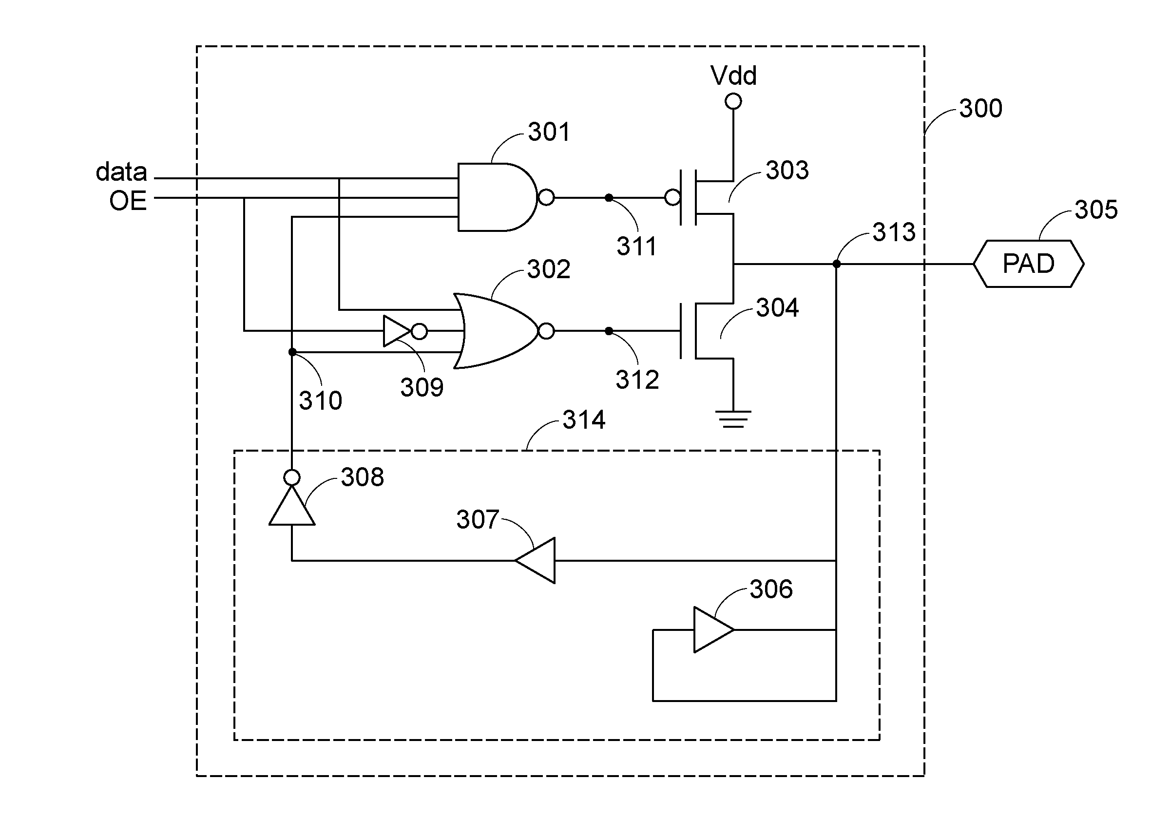
[0038]It is to be noted that the main function of the weak buffer 306 in the present invention is to maintain the high level or the low level of the output node when the pulling high capability or the pulling low capability of the tri-state I / O port 300 is turned off. Moreover, even when the outputs of the tri-state I / O port 300 and other tri-state I / O port are at different digital state, they would not suffer from the large current which flows from the power source Vdd and goes through transistors to the ground as mentioned in the prior art because the weak buffer 306 has a high impedance. In another word, when outputs of the tri-state I / O port 300 and the other tri-state I / O port are at different digital state and bus mastering switches from the tri-state I / O port 300 to the other tri-state I / O port, they would not break down because mostly the output of these tri-state I / O port are at a weak high level or at a weak low level. A turn around time in the prior art is thus not needed...

second embodiment

[0045]It is to be noted that the main function of the weak high buffer in the present invention is to maintain the high level of the output node when the pulling high capability of the tri-state I / O port 400 is turned off. Moreover, even when the outputs of the tri-state I / O port 400 and other tri-state I / O port are at different digital state, they would not suffer from the large current which flows from the power source Vdd and goes through transistors to the ground as mentioned in the prior art because the weak high buffer 406 has a high impedance. In another word, when outputs of the tri-state I / O port 400 and the other tri-state I / O port are at different digital state and bus mastering switches from the tri-state I / O port 400 to the other tri-state I / O port, they would not break down because mostly the outputs of these tri-state I / O port are at a weak high level. A turn around time in the prior art is thus not needed and the design of the tri-state I / O port 400 not only increase...

third embodiment

[0052]It is to be noted that the main function of the weak low buffer 506 in the present invention is to maintain the low level of the output node when the pulling low capability of the tri-state I / O port 500 is turned off. Moreover, even when the outputs of the tri-state I / O port 500 and other tri-state I / O port are at different digital state, they would not suffer from the large current which flows from the power source Vdd and goes through transistors to the ground as mentioned in the prior art because the weak low buffer 506 has a high impedance. In another word, when outputs of the tri-state I / O port 500 and the other tri-state I / O port are at different digital state and bus mastering switches from the tri-state I / O port 500 to the other tri-state I / O port, they would not break down because mostly the outputs of these tri-state I / O port are at a weak low level. A turn around time in the prior art is thus not needed and the design of the tri-state I / O port 500 not only increases...


PUM


Abstract

The present invention discloses a tri-state I/O port. The tri-state I/O port comprises a tri-state logic block, a weak buffer and a delay block. The input terminals of the tri-state logic block are connected to data and OE (output enable) signals. When OE signal is enabled, the output terminal of the tri-state I/O block is pulled high when the data is high while the output terminal is pulled low when the data is low. The input terminal and the output terminal of the weak buffer are connected to the output terminal of the tri-state logic block. And the input terminal of the delay block is connected to the output terminal of the tri-state logic block while the output terminal of the delay block is fed back to the tri-state logic block. When the output terminal of the tri-state logic block is low to high/high to low, the weak buffer is active and maintains the output terminal of the tri-state logic block weak high/low while the delay block turns off the pull high/low function of the tri-state logic block.

Description

FIELD OF THE INVENTION[0001]The present invention relates to a design of a tri-state I / O port, and more particularly to the design of a tri-state I / O port without a turn around time.BACKGROUND OF THE INVENTION[0002]Nowadays in the design of microprocessors and electronic systems, the protocol of data transmission regulates that when bus mastering switches, a turn around time is added in case of bus contention.[0003]Refer to FIG. 1, which illustrates a turn around time which prevents bus contention. A and B represent A drive and B drive respectively wherein A drive and B drive both adopt tri-state I / O ports and share bus 10. A_OE and B_OE represent output enable signal of A drive and output enable signal of B drive respectively. During period 11, A_OE is high which represents that A drive is enabled and transmits data or commands through bus 10. And period 12 shows a turn around time which prevents bus contention when bus mastering of bus 10 switches from A drive to B drive. During p...

Claims


Application Information

Patent Timeline
Patent Type & Authority Applications(United States)
IPC IPC(8): G01R31/28
CPCG06F13/4072
Inventor CHUANG, SHIH-JEN
Owner RDC SEMICON CO LTD
Why Eureka
Try Eureka