Method for Machining Chamfer Portion of Semiconductor Wafer and Method for Correcting Groove Shape of Grinding Stone

Active Publication Date: 2009-06-25
SHIN-ETSU HANDOTAI CO LTD
View PDF5 Cites 17 Cited by
  • Summary
  • Abstract
  • Description
  • Claims
  • Application Information

AI Technical Summary

Benefits of technology

[0008]According to the present invention, there is provided a method for machining a chamfer portion of a semiconductor wafer that is a method for subjecting a roughly ground chamfer portion of a semiconductor wafer to helical grinding by relatively inclining the wafer and a second grinding stone to perform precise grinding, comprising: forming an edge portion of a discoid truer into a vertically asymmetrical groove shape of a first grinding stone by using the first grinding stone having a vertically asymmetrical groove formed on a periphery thereof to grind the edge portion of the truer without being relatively inclined; forming a groove on a periphery of the second grinding stone by relatively inclining the truer and the second grinding stone to subject the second grinding stone to helical grinding; and precisely grinding the chamfer portion of the wafer based on helical grinding by relatively inclining the semiconductor wafer with respect to a direction of the groove formed on the periphery of the second grinding stone.
[0019]When the present invention is applied, each of the upper and lower angles of the chamfer portion becomes very close to 22 degrees as a general target, thereby obtaining the chamfer portion having the substantially vertical symmetrical shape can be machined.

Problems solved by technology

However, when a mechanical damage in the chamfer portion is deep, a damage or a grinding striation remains even though mirror edge polishing is performed, which results in a factor of particle generation.
However, if the chamber portion of the wafer is subjected to helical grinding by using the resin grinding stone as explained above, a reduction in damages in the chamfer portion of the wafer and an increase in a grinding stone life can be achieved, whereas there is a problem that vertical symmetry of the chamfer portion of the wafer considerably collapses.

Method used


Image

  • Method for Machining Chamfer Portion of Semiconductor Wafer and Method for Correcting Groove Shape of Grinding Stone
  • Method for Machining Chamfer Portion of Semiconductor Wafer and Method for Correcting Groove Shape of Grinding Stone
  • Method for Machining Chamfer Portion of Semiconductor Wafer and Method for Correcting Groove Shape of Grinding Stone

Examples


example 1

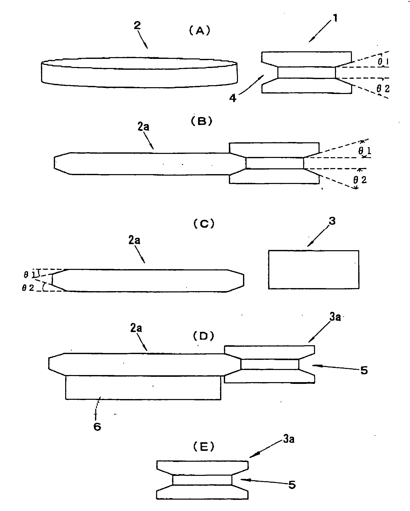
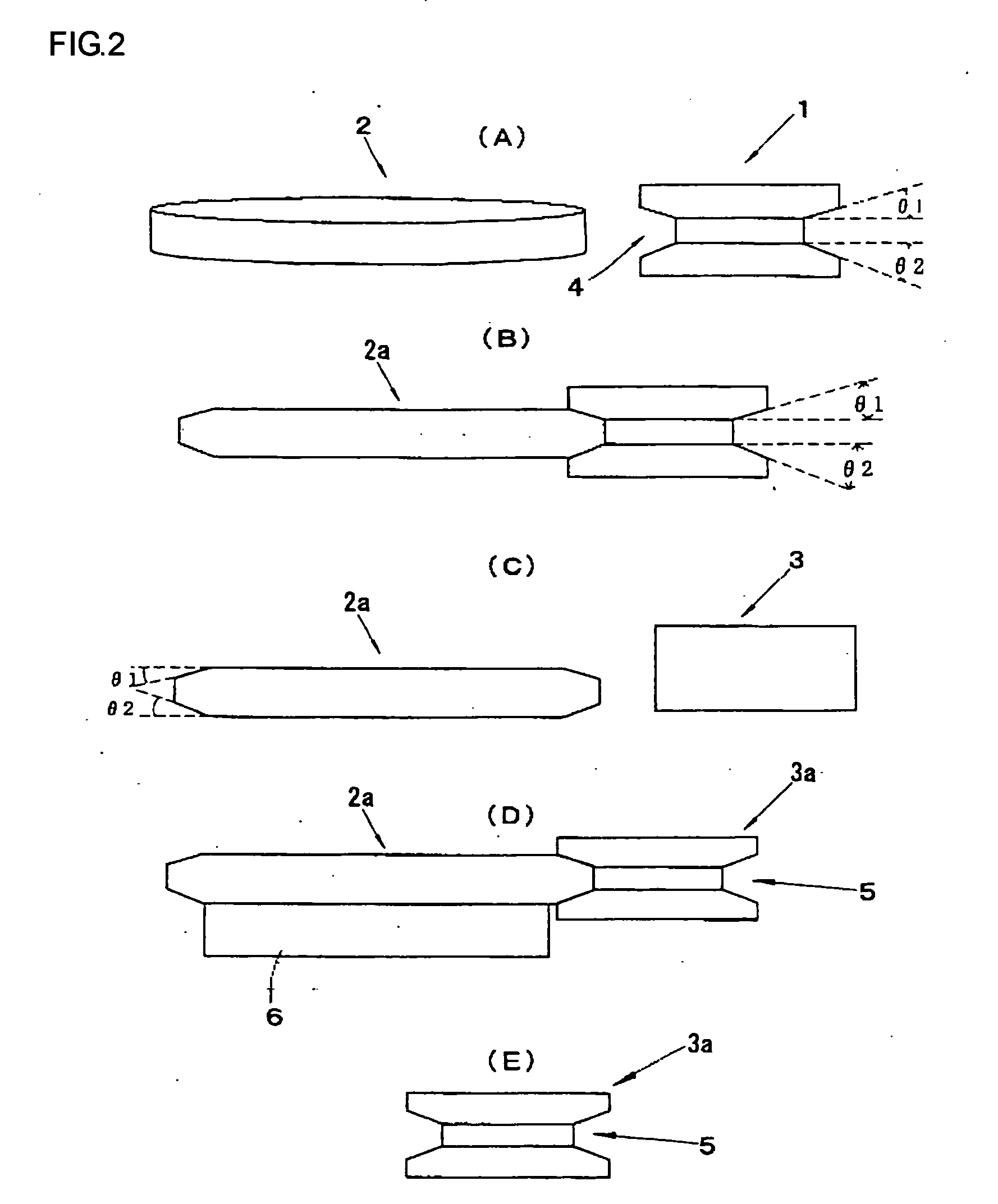
[0058]A metal grinding stone (main components: a metal powder (Fe, Cr, Cu), diamond abrasive grains) having a vertically asymmetrical groove with an upper angle of 22 degrees and a lower angle of 21 degrees formed on a periphery thereof was prepared as a prototype. An edge portion of a discoid truer was ground to be formed into a groove shape of the metal grinding stone by the groove of the metal grinding stone without being relatively inclined. A configuration of the truer is as shown in the following Table 1.

TABLE 1ConstituentsComponent namesContents (wt %)Abrasive grainsSilicon carbide70%BinderPhenol resin28%FillerClay-based filler 1%OthersCarbon black 1%

[0059]The truer having the edge portion formed as explained above was held on an adsorption table of a helical chamfering machine, and a periphery of an obliquely attached resin grinding stone (main components: a phenol resin, diamond abrasive grains) was subjected to helical grinding, thereby forming a groove on the periphery of...


PUM

PropertyMeasurementUnit
Angleaaaaaaaaaa
Angleaaaaaaaaaa
Shapeaaaaaaaaaa

Abstract

According to the present invention, in a method for subjecting a roughly ground chamfer portion of a semiconductor wafer to helical grinding by relatively inclining the wafer and a second grinding stone to perform precise grinding, an edge portion of a discoid truer is formed into a vertically asymmetrical groove shape of a first grinding stone by using the first grinding stone having a vertically asymmetrical groove formed on a periphery thereof to grind the edge portion of the truer by the groove of the first grinding stone without being relatively inclined, a groove is formed on a periphery of the second grinding stone by relatively inclining the truer and the second grinding stone to subject the second grinding stone to helical grinding, and the chamfer portion of the wafer is precisely ground based on helical grinding by relatively inclining the semiconductor wafer with respect to a direction of the groove formed on the periphery of the second grinding stone. As a result, there is provided the method for machining a chamfer portion of the semiconductor wafer, which can machine the chamfer portion of the wafer into a vertically symmetrical shape when subjecting the chamfer portion of the semiconductor wafer to helical grinding, e.g. a resin grinding stone and the like.

Description

TECHNICAL FIELD[0001]The present invention relates to a method for precisely grinding a chamfer portion of a semiconductor wafer, e.g., a silicon wafer, based on helical grinding.BACKGROUND ART[0002]A semiconductor wafer, e.g., a silicon wafer, for use in fabrication of a semiconductor device and the like is chamfered by grinding an edge portion in order to avoid chipping due to handling, and also subjected to mirror edge polishing based on polishing as a particle generation countermeasure in a device process in recent years. However, when a mechanical damage in the chamfer portion is deep, a damage or a grinding striation remains even though mirror edge polishing is performed, which results in a factor of particle generation.[0003]Thus, as a method for reducing a mechanical damage in the chamfer portion, there is a method for performing so-called helical grinding with respect to a chamfer portion of a wafer, for example, while inclining a resin bond grinding stone (a resin grinding...

Claims


Application Information

Patent Timeline
IPC IPC(8): B24B9/06
CPCB24B9/065H01L21/02021B24B53/07H01L21/304B24B9/00
Inventor YAMAZAKI, EIICHISEKINE, TAKASHI
Owner SHIN-ETSU HANDOTAI CO LTD
Why Eureka
Try Eureka