Memory cell with planarized carbon nanotube layer and methods of forming the same

a carbon nanotube and memory cell technology, applied in nanoinformatics, thermoelectric devices, instruments, etc., can solve the problem of technical challenges in fabricating memory devices from rewitable resistivity-switching materials

Inactive Publication Date: 2009-07-02
SANDISK TECH LLC
View PDF41 Cites 111 Cited by
  • Summary
  • Abstract
  • Description
  • Claims
  • Application Information

AI Technical Summary

Benefits of technology

[0010]In a fourth aspect of the invention, a memory cell is provided that includes (1) a first conductor; (2) a reversible resistance-switching element including carbon nano-tube (CNT) material fabricated above the first conductor, wherein the reversible resistance-switching element comprises a plurality of CNTs; (3) a dielectric material disposed between the CNTs, such that the plurality of CNTs are exposed in a planar surface of the reversible resistance-switching element; (4) a diode formed above the first conductor; and (5) a second conductor formed above the reversible resistance-switching element and the diode.
[0011]In a fifth aspect of the invention, a plurality of nonvolatile memory cells is provided that includes (1) a first plurality of substantially parallel, substantially coplanar conductors extending in a first direction; (2) a plurality of diodes; (3) a plurality of reversible resistance-switching elements, wherein each reversible resistance-switching element comprises a plurality of carbon nano-tubes (CNTs) and a dielectric material disposed between the CNTs, such that the plurality of CNTs are exposed in a planar surface of the reversible resistance-switching element; and (4) a second plurality of substantially parallel, substantially coplanar conductors extending in a second direction different from the first direction. In each memory cell, one of the diodes is formed in series with one of the reversible resistance-switching elements, disposed between one of the first conductors and one of the second conductors. Each reversible resistance-switching element in

Problems solved by technology

However, fabricating memory devices from rewritable resistivity-switching materials is technically challenging; an

Method used


Image

  • Memory cell with planarized carbon nanotube layer and methods of forming the same
  • Memory cell with planarized carbon nanotube layer and methods of forming the same
  • Memory cell with planarized carbon nanotube layer and methods of forming the same

Examples


first exemplary embodiment

of a Memory Cell

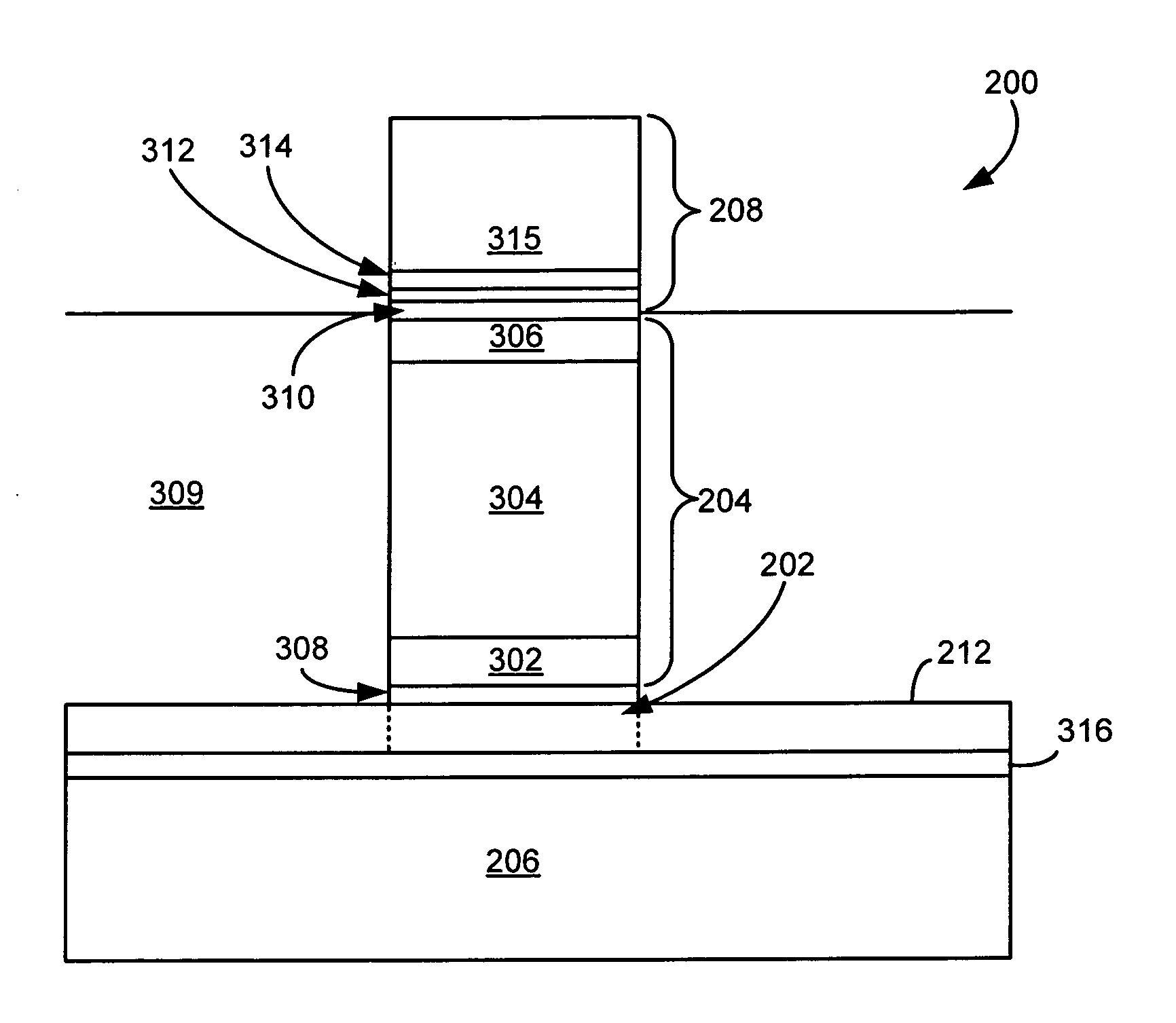
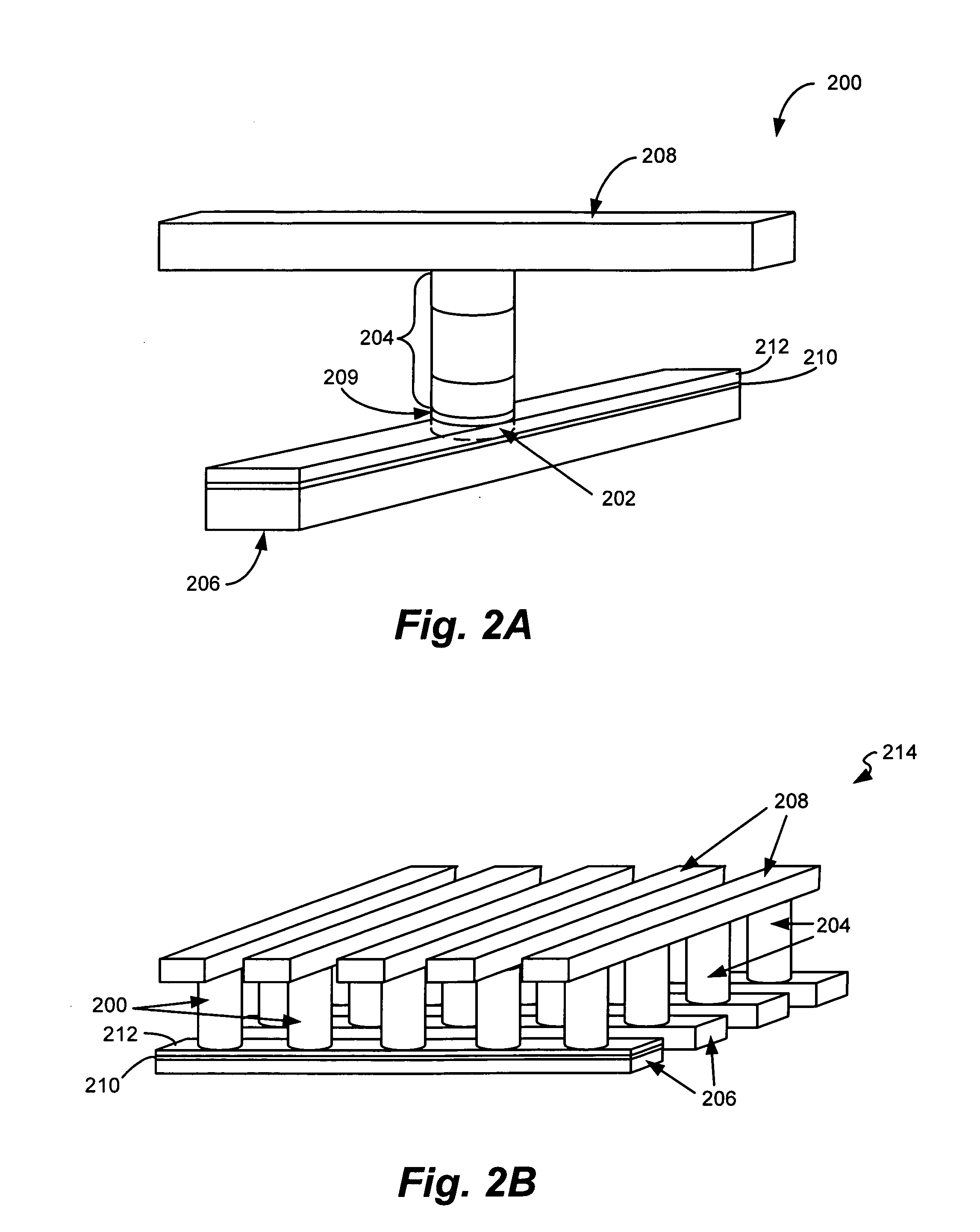
[0036]FIG. 2A is a simplified perspective view of a first embodiment of a memory cell 200 provided in accordance with the present invention. With reference to FIG. 2A, the memory cell 200 includes a reversible resistance-switching element 202 (shown in phantom) coupled in series with a diode 204 between a first conductor 206 and a second conductor 208. In some embodiments, a barrier layer 209 such as titanium nitride, tantalum nitride, tungsten nitride, etc., may be provided between the reversible resistance-switching element 202 and the diode 204.

[0037]As will be described further below, the reversible resistance-switching element 202 is selectively formed so as to simplify fabrication of the memory cell 200. In at least one embodiment, the reversible resistance-switching element 202 includes at least a portion of a CNT material formed on a CNT seeding layer such as titanium nitride, tantalum nitride, nickel, cobalt, iron or the like. For example, a titanium or tant...


PUM


Abstract

In some aspects, a method of fabricating a memory cell is provided that includes (1) fabricating a first conductor above a substrate; (2) fabricating a carbon nano-tube (CNT) material above the first conductor; (3) depositing a dielectric material onto a top surface of the CNT material; (4) planarizing the dielectric material to expose at least a portion of the CNT material; (5) fabricating a diode above the first conductor; and (6) fabricating a second conductor above the CNT material and the diode. Numerous other aspects are provided.

Description

CROSS REFERENCE TO RELATED APPLICATIONS[0001]The present application is related to the following patent applications which are hereby incorporated by reference herein in their entirety for all purposes:[0002]U.S. patent application Ser. No. ______, filed on even date herewith and titled “MEMORY CELL THAT EMPLOYS A SELECTIVELY FABRICATED CARBON NANO-TUBE REVERSIBLE RESISTANCE-SWITCHING ELEMENT AND METHODS OF FORMING THE SAME” (Docket No. SD-MXD-348).[0003]U.S. patent application Ser. No. ______, filed on even date herewith and titled “MEMORY CELL THAT EMPLOYS A SELECTIVELY FABRICATED CARBON NANO-TUBE REVERSIBLE RESISTANCE-SWITCHING ELEMENT FORMED OVER A BOTTOM CONDUCTOR AND METHODS OF FORMING THE SAME” (Docket No. SD-MXD-351).FIELD OF THE INVENTION[0004]The present invention relates to non-volatile memories and more particularly to a memory cell that employs a selectively fabricated carbon nano-tube (CNT) reversible resistance-switching element formed over a bottom conductor and meth...

Claims


Application Information

Patent Timeline
IPC IPC(8): H01L21/8229H01L51/30
CPCB82Y10/00H01L27/2481B82Y40/00G11C13/0014G11C13/025G11C2213/71G11C2213/72H01L21/31053H01L27/1021H01L27/285H01L45/04H01L51/0048H01L51/0587H01L51/0591H01L51/0595H01L45/1233H01L45/149H01L45/1616H01L27/2409B82Y30/00H10B63/84H10B63/20H10N70/20H10N70/8845H10N70/023H10N70/826H10K19/202H10K85/221H10K10/29H10K10/50H10K10/701Y10S977/762
Inventor SCHRICKER, APRILCLARK, MARKHERNER, BRADTANAKA, YOICHIRO
Owner SANDISK TECH LLC
Why Eureka
Try Eureka