Incorporating reflective layers into LED systems and/or components

a reflective layer and led system technology, applied in the field of high-intensity light-emitting diodes, can solve the problems of not being very reflective, not optimized for its optical properties, and printed circuit boards contributing to optical losses

Inactive Publication Date: 2009-07-02
GE LIGHTING SOLUTIONS LLC
View PDF12 Cites 51 Cited by
  • Summary
  • Abstract
  • Description
  • Claims
  • Application Information

AI Technical Summary

Problems solved by technology

Disadvantageously, the printed circuit board can contribute to optical losses by partially absorbing light that impinges upon the printed circuit board.
In conventional printed circuit boards for electronic applications, the solder mask layer is not optimized for its optical properties, and is thus not very reflective.
White solder masks have certain disadvantages for some high brightness light emitting packages.
If 50% of the visible light produced by the light emitting package impinges on the printed circuit board, this reflectance corresponds to optical losses of around 10% or higher due to absorption in the printed circuit board.
The relatively low reflectance of white solder masks for blue, violet, or ultraviolet wavelength light degrades the light output efficiency of these packages.
However, incorporating a metallic reflector, which is generally electrically conductive, into a solder mask is problematic since the solder mask is in contact with or in proximity to the printed circuitry and electronic component leads.

Method used


Image

  • Incorporating reflective layers into LED systems and/or components
  • Incorporating reflective layers into LED systems and/or components
  • Incorporating reflective layers into LED systems and/or components

Examples


Embodiment Construction

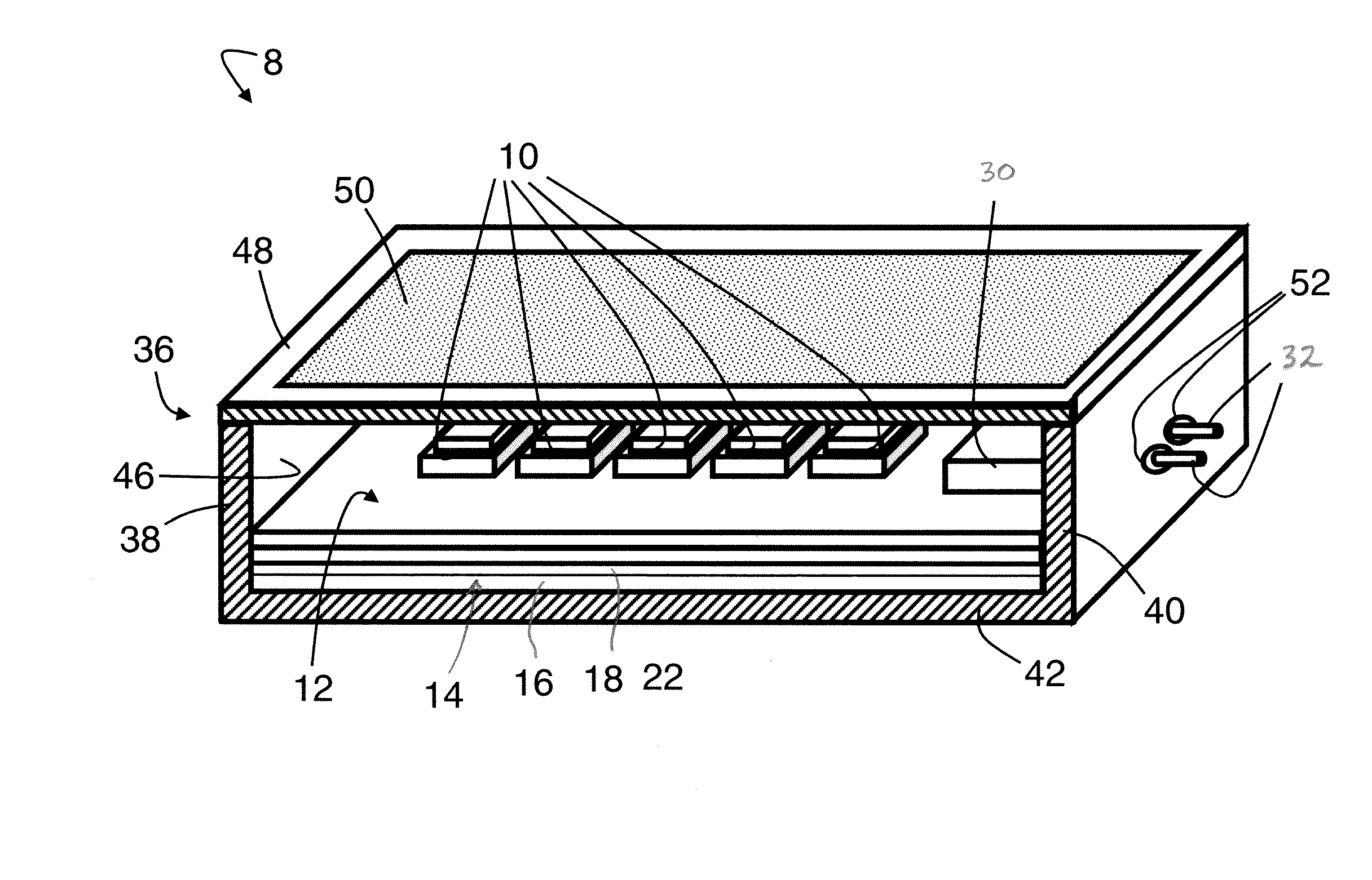
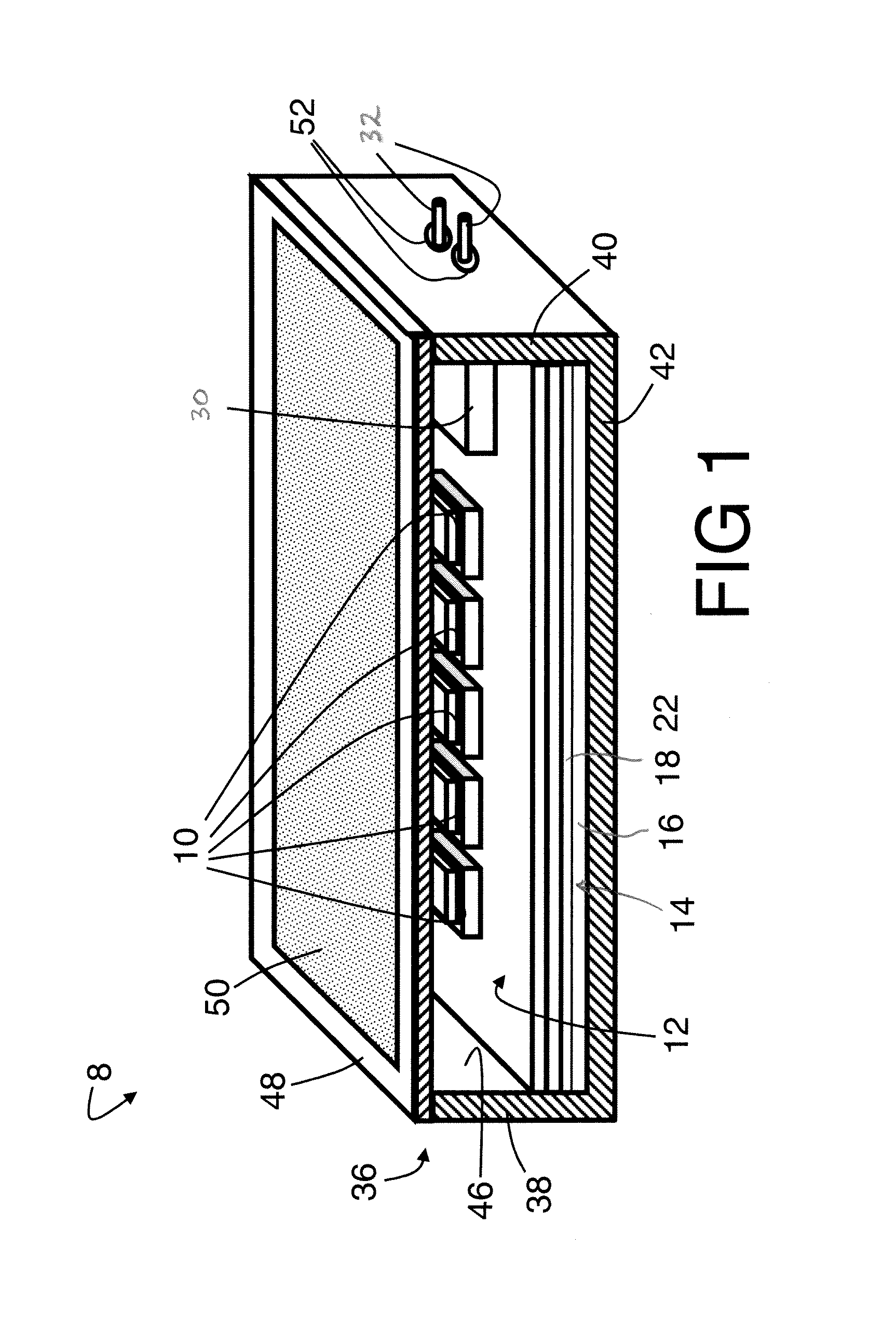
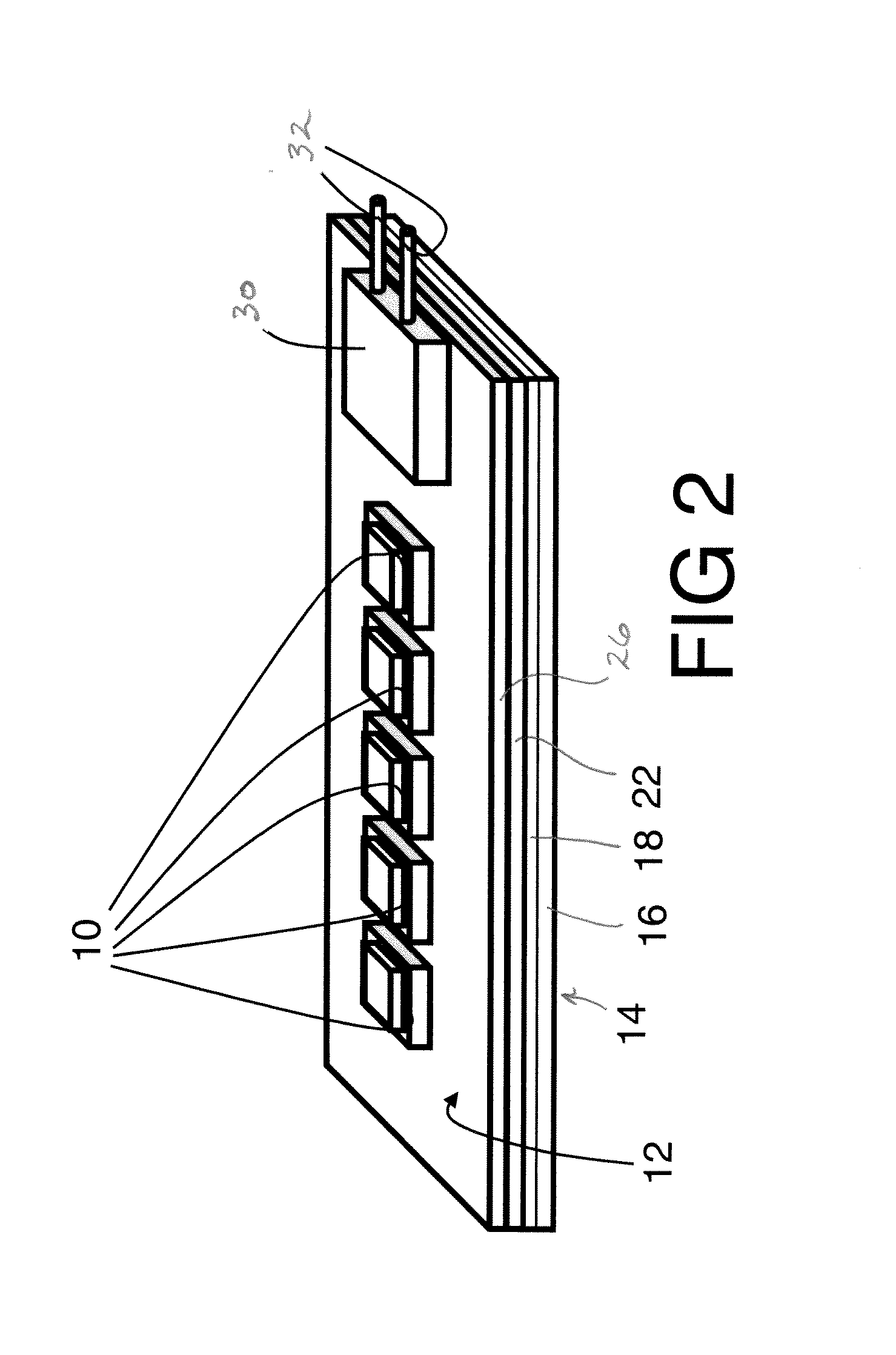
[0019]With reference to FIGS. 1-3, a light emitting apparatus 8 includes a plurality of light emitting chips 10 disposed on a support, which in the depicted embodiment is a printed circuit board 12. The illustrated printed circuit board 12 includes an electrically insulating board 14, which in the illustrated embodiment includes a conductive metal core 16 and an insulating layer 18 made of a fiberglass resin or another electrically insulating material. In some embodiments, the conductive metal core 16 is omitted: for example, the electrically insulating board may be a fiberglass resin board without a metal core. Electrically conductive printed circuitry 20 (shown in FIG. 3) is disposed on the insulating layer 18 of the insulating board 14. A solder mask 22 is disposed on the insulating board 16 and includes openings or vias 24 (shown in FIG. 3) through which the light emitting chips 10 electrically contact the printed circuitry 20. A highly reflective layer 26, which can be a highly...


PUM

PropertyMeasurementUnit
reflectanceaaaaaaaaaa
wavelength rangeaaaaaaaaaa

Abstract

A light emitting apparatus includes a support having circuitry disposed thereon, at least one light emitting diode (LED) chip mounted on the support and in electrical communication with the circuitry and a reflective layer on the support adjacent the at least one chip.

Description

BACKGROUND[0001]The present invention relates to the lighting arts. It especially relates to high intensity light emitting diode packages, components, apparatuses, and so forth, and will be described with particular reference thereto. However, the invention will also find application in conjunction with other solid state light emitters such as vertical cavity surface emitting lasers.[0002]High brightness light emitting packages typically employ a plurality of light emitting diode chips, surface emitting laser chips, organic light emitter chips, or the like. To mechanically support the chips and to electrically interconnect the chips, in some light emitting packages the light emitting chips are disposed on a printed circuit board. The printed circuit board can also support and electrically incorporate discrete electronic components, application-specific integrated circuits (ASICs), programmable microprocessors, or the like, for providing input power conditioning, light output control...

Claims


Application Information

Patent Timeline
Patent Type & Authority Applications(United States)
IPC IPC(8): H01L33/00F21V7/22H01L21/027H05K3/32
CPCF21K9/00H05K3/28H05K3/285Y10T29/4913H05K2201/10106H05K2201/2054H05K2201/015F21K9/64
Inventor WEAVER, JR., STANTON E.REGINELLI, JAMES
Owner GE LIGHTING SOLUTIONS LLC
Why Eureka
Try Eureka