Communication system between a first and a second synchronous device that are uncorrelated in time

a communication system and synchronous device technology, applied in the field of communication systems, can solve problems such as high power consumption of communication circuits

Active Publication Date: 2009-07-02
STMICROELECTRONICS SRL
View PDF11 Cites 26 Cited by
  • Summary
  • Abstract
  • Description
  • Claims
  • Application Information

AI Technical Summary

Benefits of technology

[0029]Even advantageously under several aspects, also this known system require the definition of a dedicated clo

Problems solved by technology

In this field, synchronization is a key issue for modern integrated systems where the distribution of a global clock signal is not possible or not advis

Method used


Image

  • Communication system between a first and a second synchronous device that are uncorrelated in time
  • Communication system between a first and a second synchronous device that are uncorrelated in time
  • Communication system between a first and a second synchronous device that are uncorrelated in time

Examples


Embodiment Construction

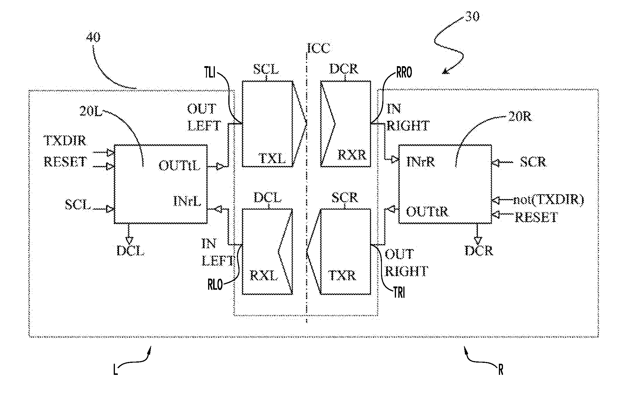
[0052]With reference to such figures, and in particular to FIG. 3, a communication system between independently clocked devices, in particular chips, globally indicated at 30, hereinafter briefly called the system 30.

[0053]The system 30 provides for the communication between a first or left chip (L) and a second or right chip (R) and comprises, for each chip, a transmitter, TXL and TXR, and a receiver, RXL and RXR, connected to each other in a crossed way in correspondence of an inter-chip communication channel ICC, indicated with a dotted line in FIG. 3. In particular, the transmitter TXL of the left chip L is connected to the receiver RXR of the right chip R and, similarly, the transmitter TXR of the right chip R is connected to the receiver RXL of the left chip L.

[0054]The transmitters TXL and TXR also have respective clock terminals receiving system clock signals SCL and SCR, while the receivers RXL and RXR have respective clock terminals receiving delayed clock signals DCL and ...


PUM


Abstract

A communication system includes first and second independently clocked devices, comprising, for each device, a transmitter and a receiver connected to each other in a crossed way in correspondence of an inter-chip communication channel. The communication system further comprises a synchronizer in turn including at least a first and a second synchronization block, having respective input terminals connected to the receivers and respective output terminals connected to the transmitters and comprising at least: a test pattern generator that generates a programmable test pattern signal; a pattern detector to check a matching between stored and received test pattern signals and thus lock corresponding clock phases of the synchronization blocks in case of positive result of this check; and a delay block able to change the clock phases until a synchronized condition of the synchronization blocks is verified, this synchronized condition corresponding to a matching between stored and received test pattern signals.

Description

BACKGROUND[0001]1. Technical Field[0002]The present invention relates to a communication system between first and second independently clocked devices, for example, first and second chips.[0003]The invention particularly, but not exclusively, relates to a chip-to-chip communication system for a stacked device, i.e., a device comprising at least two chips assembled in a three-dimensional (3D) stacking configuration and the following description is made with reference to this field of application for convenience of explanation only.[0004]2. Description of the Related Art[0005]As it is well known, the development of stacking technology for heterogeneous device integration has recently increased in importance.[0006]Stacking of chips, in which two or more integrated circuits or ICs of different types are placed one on the top of the other in a same package, is an alternative to silicon integration and provides improvements at the system design level in terms of size, cost, speed, power c...

Claims


Application Information

Patent Timeline
IPC IPC(8): H04B3/46
CPCH04L7/0037H04L7/10
Inventor MAGAGNI, LUCACICCARELLI, LUCAFAZZI, ALBERTOCANEGALLO, ROBERTOGUERRIERI, ROBERTO
Owner STMICROELECTRONICS SRL
Why Eureka
Try Eureka