Method for manufacturing a semiconductor device

a manufacturing method and technology for semiconductor devices, applied in semiconductor/solid-state device manufacturing, basic electric elements, electric devices, etc., can solve the problems of inability to supply silylating agent further into the pores, and inability to completely repair damage in the pores of the film, etc., to achieve suppressed wiring resistance and insulating film capacity, excellent capability, and high speed

Active Publication Date: 2009-07-02
PANNOVA SEMIC
View PDF6 Cites 18 Cited by
  • Summary
  • Abstract
  • Description
  • Claims
  • Application Information

AI Technical Summary

Benefits of technology

[0014]In view of the above problems, it is an object of the present invention to provide a method for manufacturing a semiconductor device having a low dielectric constant film having excellent capability even if the low dielectric constant film is damaged during a manufacturing process.
[0041]A twenty-third manufacturing method of the semiconductor device of the present invention further includes the step of after the step (c), forming in the low dielectric constant film a recess formed by a via hole and a wiring groove connecting to the via hole, and embedding a metal in the recess to simultaneously form a via plug and a metal wiring. In this case, since the low dielectric constant film is silylated before being processed, damages that are conventionally generated by formation of a recess in the low dielectric constant film can be suppressed. As a result, a high-strength low dielectric film having excellent capability is obtained and the wiring resistance and the insulating film capacity are suppressed, thereby implementing a reliable semiconductor device having a dual damascene wiring and capable of operating at a high speed even when the semiconductor device is reduced in dimensions.

Problems solved by technology

However, the conventional method for recovering the damages generated by formation of the recess has the following problems.
As a result, the silylating agent cannot be supplied further into the pores.
The silylating agent is less likely to be supplied deep into the pores due to the small pore diameter, or the silylating agent cannot be supplied further into the pores when the silylating agent itself reacts with OH groups.
As described above, in the case of a porous film, damages in the pores of the film cannot be completely repaired even by the conventional silylation process.
Moreover, although the mechanical strength of the low dielectric constant film is improved by the cure process, the principal chain and side chains in the low dielectric constant film are broken by the cure process.
Since not all of the broken part of the principal chain and the broken side chains are recombined, damages are generated in the low dielectric constant film.
However, the same problems as those described above occur in the case of a porous film having a pore diameter of about several nanometers or more.

Method used


Image

  • Method for manufacturing a semiconductor device
  • Method for manufacturing a semiconductor device
  • Method for manufacturing a semiconductor device

Examples


first embodiment

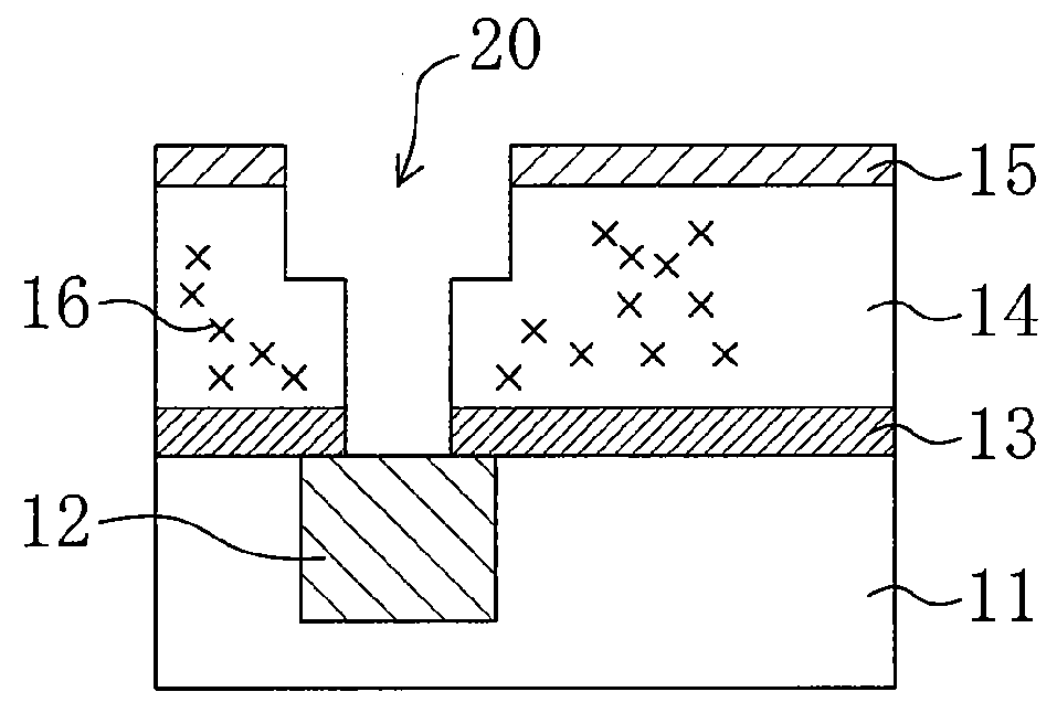
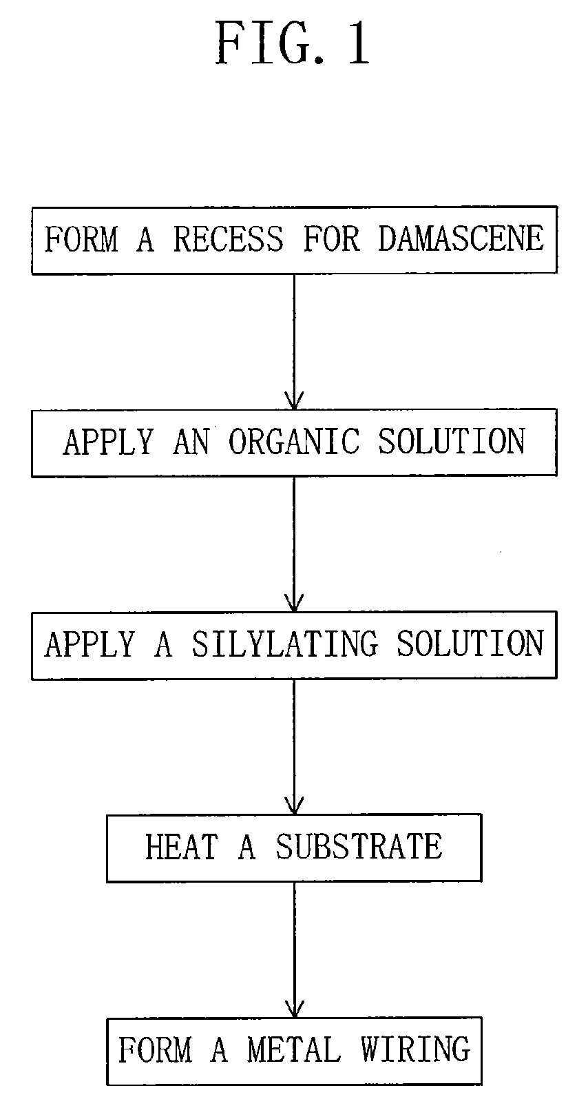
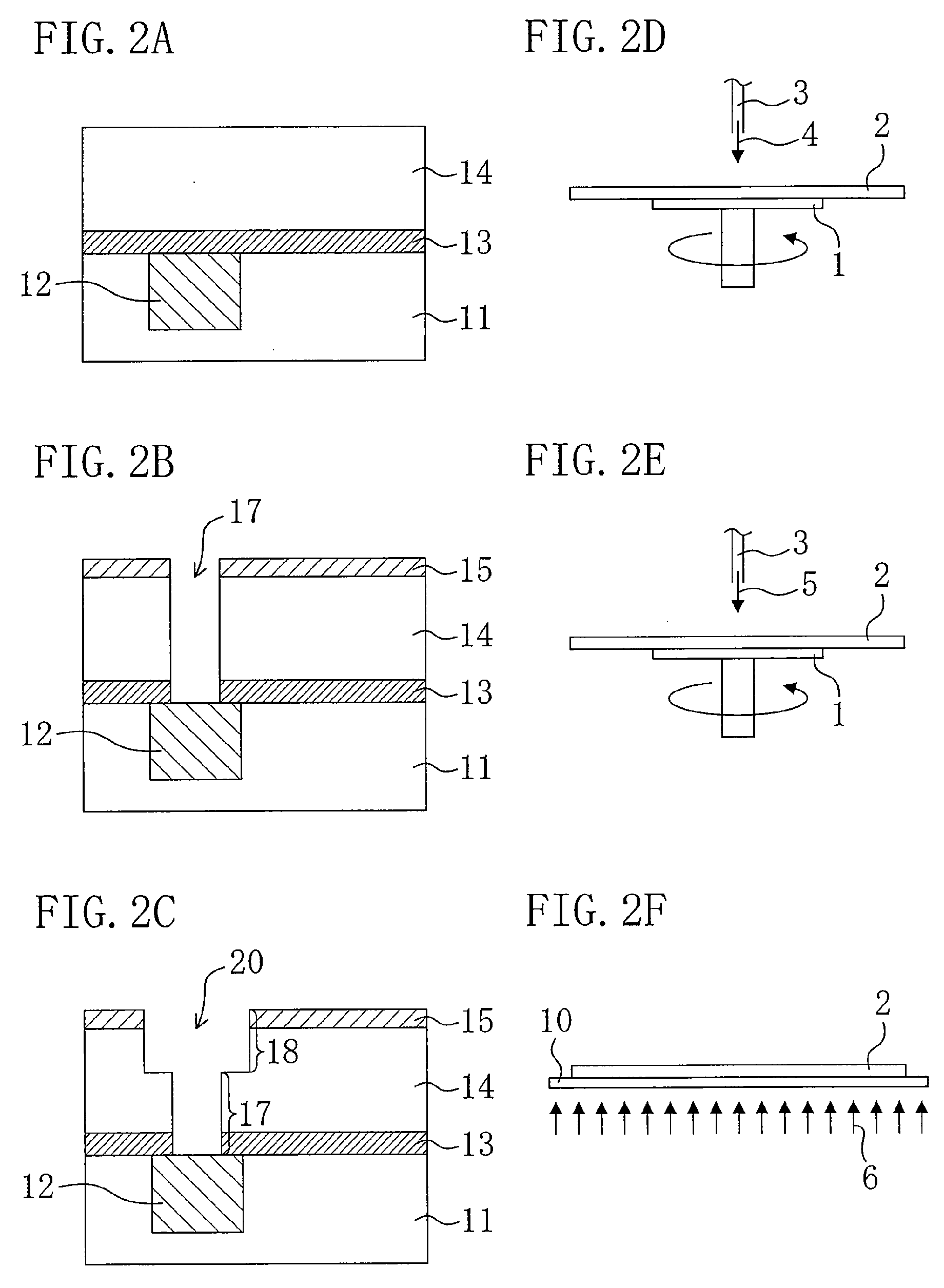
[0053]Hereinafter, a method for manufacturing a semiconductor device according to a first embodiment of the present invention will be described with reference to the figures. FIG. 1 shows a process sequence according to the method for manufacturing a semiconductor device according to the first embodiment. FIGS. 2A through 2F are diagrams illustrating the method for manufacturing a semiconductor device according to the first embodiment. In the first embodiment, description is given to the case where a multilayer wiring structure made of, for example, Cu is formed by using a dual damascene method.

[0054]First, as shown in FIGS. 1 and 2A, an interlayer insulating film 11 having a wiring groove is formed over a semiconductor substrate (not shown) having required semiconductor elements formed thereon. The interlayer insulating film 11 is made of, for example, an NSG (Non Silicate Glass) film which is a thermal oxide film. A lower wiring 12 of, for example, Cu is formed by embedding Cu in ...

second embodiment

[0082]Hereinafter, a method for manufacturing a semiconductor device according to a second embodiment of the present invention will be described. FIGS. 6A and 6B are diagrams illustrating the method for manufacturing a semiconductor device according to the second embodiment. In the second embodiment, description will be given to the case where a multilayer wiring structure made of Cu or the like is formed by using a single damascene method. Only the differences from the first embodiment will be described herein briefly.

[0083]As shown in FIG. 6A, an interlayer insulating film 11 made of, for example, an NSG film, is formed over a semiconductor substrate (not shown) having required semiconductor elements formed thereon. A lower wiring 12 made of Cu or the like is then formed in the interlayer insulating film 11. An etching stopper film 13 and a first low dielectric constant film 14a are then sequentially formed over the lower wiring 12 and the interlayer insulating film 11. A cap film...

third embodiment

[0089]Hereinafter, a method for manufacturing a semiconductor device according to a third embodiment of the present invention will be described. FIG. 7 shows a process sequence according to the manufacturing method of the semiconductor device of the third embodiment. In the third embodiment, a porous SiOC film is used as an example.

[0090]As shown in FIG. 7, a low dielectric constant insulating film (low dielectric constant film) is first formed on a semiconductor substrate having required semiconductor elements formed thereon. The low dielectric constant film is then reformed (UV cure or EB cure) by applying UV beams or electron beams (EB) to the semiconductor substrate while heating the semiconductor substrate. Although this reforming process increases the mechanical strength of the low dielectric constant film, film damages are generated in the low dielectric constant film. These film damages are dangling bonds, Si—H, and Si—OH formed at terminal ends of the low dielectric constan...


PUM

PropertyMeasurementUnit
dielectric constantaaaaaaaaaa

Abstract

A method for manufacturing a semiconductor device includes the steps of: (a) forming a low dielectric constant film over a semiconductor substrate; (b) forming a recess in the low dielectric constant film; (c) after the step (b), sequentially performing the steps of (c1) applying an organic solution to the low dielectric constant film and (c2) silylating the low dielectric constant film with a silylating solution; and (d) after the step (c), embedding a metal in the recess to form at least one of a via plug and a metal wiring in the low dielectric constant film. Performing the step (c1) before the step (c2) improves a penetration property of the silylating solution into the low dielectric constant film.

Description

CROSS-REFERENCE TO RELATED APPLICATIONS[0001]This application claims priority from Japanese Patent Application No. 2007-339766 filed on Dec. 28, 2007, the disclosure of which application is hereby incorporated by reference into this application in its entirety for all purposes.BACKGROUND OF THE INVENTIONRelated Art[0002]With dimensional reduction of LSI (Large Scale Integration), there has been a growing demand for further improvement in operation speed of semiconductor elements and further reduction in power consumption. In order to ensure reduction in both wiring resistance and wiring capacity in wiring formation, it has been considered to use copper (Cu) having a lower resistance than that of aluminum (Al) as a wiring material and to use a low dielectric constant insulating film having a lower relative dielectric constant k than that of a silicon oxide (SiO2) film, that is, a so-called low dielectric constant film, as a material of an insulating film between wirings. Development ...

Claims


Application Information

Patent Timeline
Patent Type & Authority Applications(United States)
IPC IPC(8): H01L21/768
CPCH01L21/02063H01L21/3105H01L21/76831H01L21/76825H01L21/76826H01L21/76814
Inventor MORINAGA, YASUNORINAKAGAWA, HIDEO
Owner PANNOVA SEMIC
Why Eureka
Try Eureka