Organic light-emitting device and method for forming the same

a light-emitting device and organic technology, applied in the direction of discharge tube luminescnet screens, discharge tube/lamp details, electric discharge lamps, etc., can solve the problems of reducing luminous efficiency, additional processes and production costs, and unprotected oled display devices are prone to rapid degradation of performance, so as to avoid moisture infiltration, increase the operational life of the device, and avoid the effect of degrading light-emitting efficiency

Active Publication Date: 2009-07-09
INNOLUX CORP
View PDF6 Cites 16 Cited by
  • Summary
  • Abstract
  • Description
  • Claims
  • Application Information

AI Technical Summary

Benefits of technology

[0007]One aspect of the present invention is to provide an organic light-emitting device without degrading light-emitting efficiency and implementing additional processes, thereby avoiding moisture infiltration and increasing the operational lifetime thereof.

Problems solved by technology

Despite their advantages, unprotected OLED display devices are prone to rapid degradation of performance due to adverse effects of oxygen and / or moisture present in the ambient environment.
However, these methods can cause additional processes and production cost, and can even reduce the luminous efficiency due to the shielding effect of the protective layer.
Therefore, there may be issues of moisture infiltration and incompatibility with some OLEDs.

Method used


Image

  • Organic light-emitting device and method for forming the same
  • Organic light-emitting device and method for forming the same
  • Organic light-emitting device and method for forming the same

Examples


Embodiment Construction

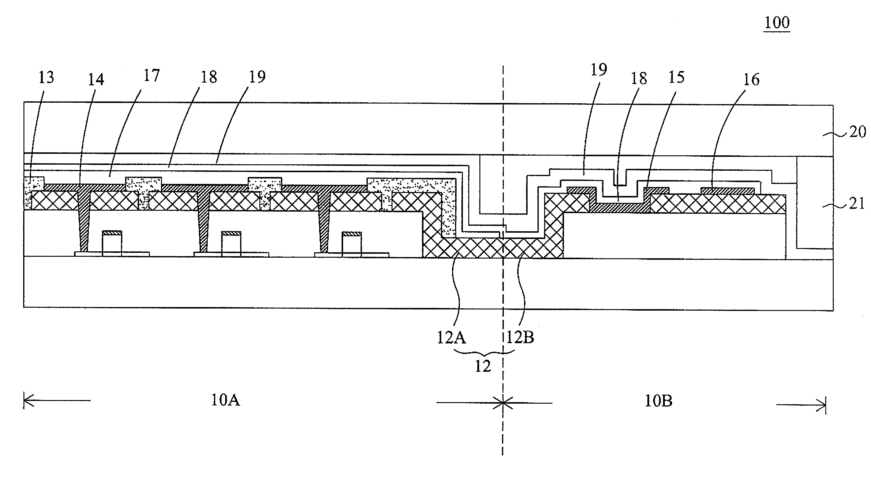
[0014]The drawings are provided for illustrative purposes only and, as such, they are not drawn to scale. The invention itself, however, in terms of both organization and method of operation, may best be understood by reference to the detailed description which follows taken in conjunction with the accompanying drawings. In the embodiments of the present invention, the same or like reference numbers will be used throughout the drawings to refer to the same or like parts.

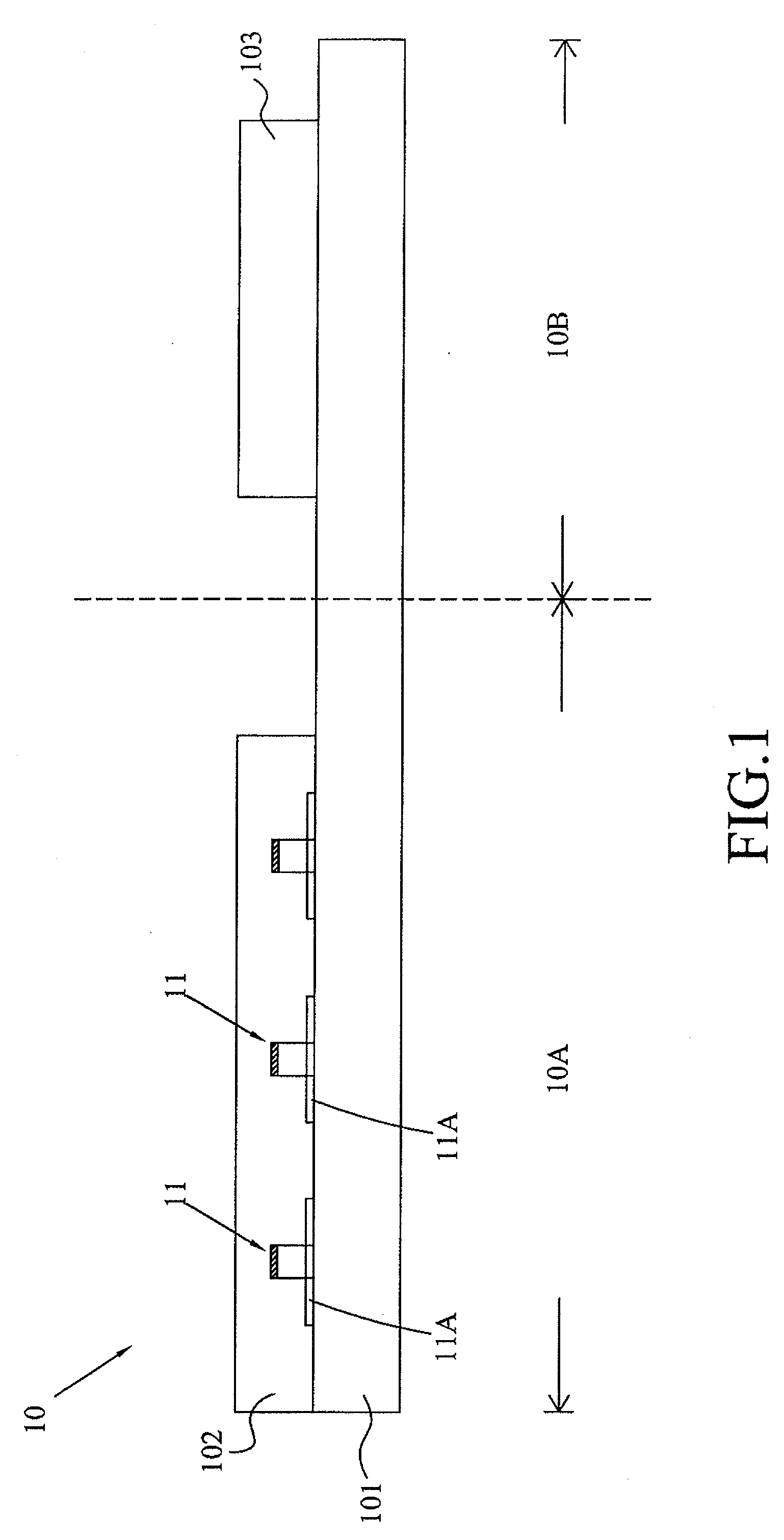
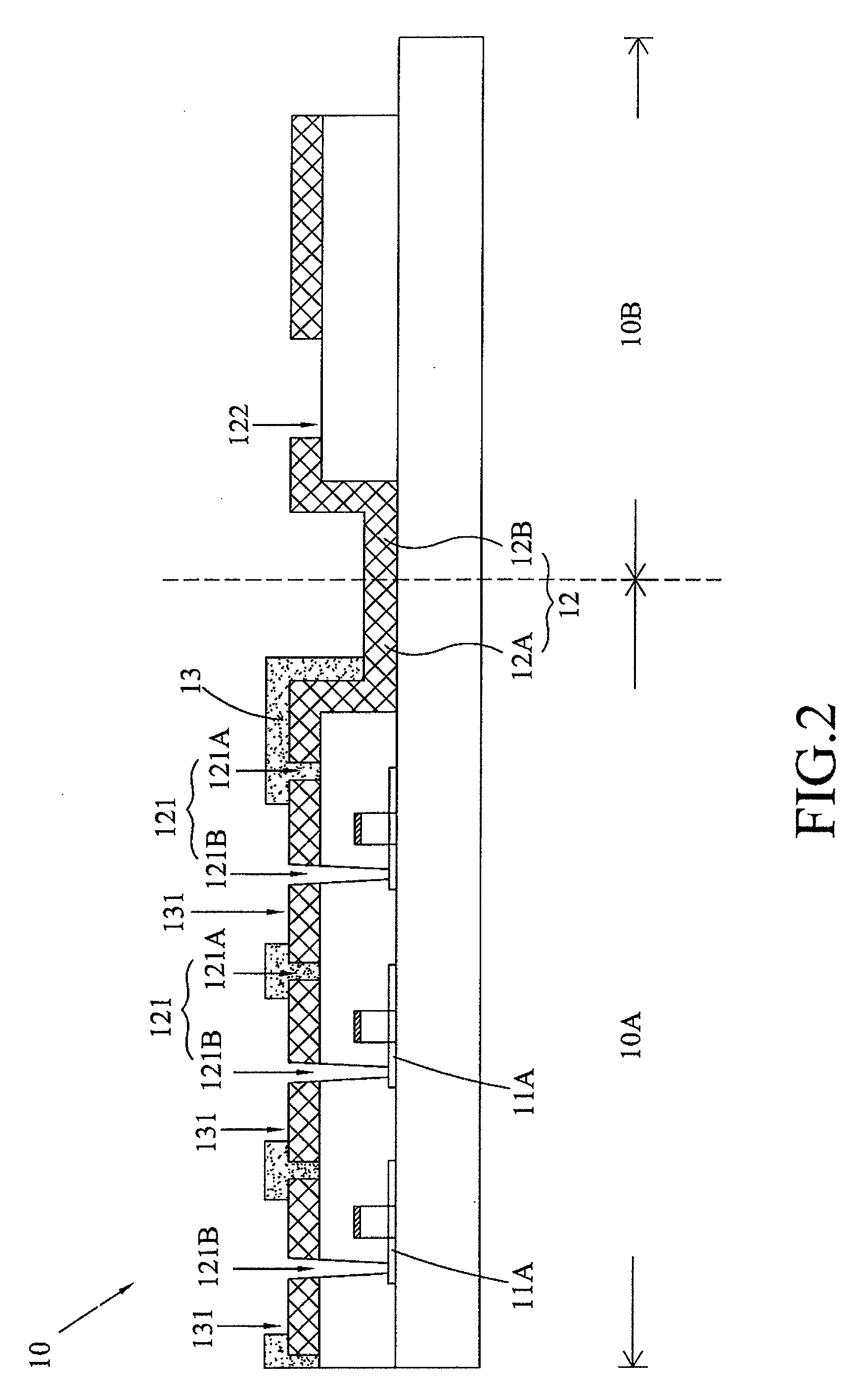
[0015]FIGS. 1-7 are cross-sectional views of organic light-emitting devices in accordance with an embodiment of the present invention.

[0016]Referring to FIG. 1, a substrate 10 has a glass substrate 101, a dielectric layer 102 and a circuit layer 103. The substrate 10 can also be divided into a pixel area 10A and a peripheral circuit area 10B. For example, the pixel area 10A generally is the center region of a display panel for displaying information, and the peripheral circuit area 10B generally is the edge region of...


PUM


Abstract

An organic light-emitting device and a method for forming the same are provided. The organic light-emitting device includes: a substrate including a pixel area and a peripheral circuit area; a passivation layer on the substrate, the passivation layer including a first part in the pixel area and a second part in the peripheral circuit area; a pixel definition layer defining a plurality of pixel openings corresponding to the pixel area of the substrate; a plurality of first electrodes in the pixel openings; an adhesion layer on the second part; an organic layer on the first electrodes; and a second electrode layer on the organic light emitting layer, wherein the second electrode extends to the peripheral circuit area to connect with the adhesion layer.

Description

CROSS REFERENCE TO RELATED APPLICATIONS[0001]This application claims the right of priority based on Taiwan Patent Application No. 097100391 entitled “organic light-emitting device and method of forming the same”, filed on Jan. 4, 2008, which is incorporated herein by reference and assigned to the assignee herein.FIELD OF THE INVENTION[0002]This invention relates to an organic light-emitting device, and more particularly, to an organic light-emitting device for protecting against external moisture and a method of forming the same.BACKGROUND OF THE INVENTION[0003]Organic light-emitting diode (OLED) devices, also referred to as organic electroluminescent (EL) devices, have numerous well known advantages over other flat-panel display devices currently in the market place.[0004]Applications of OLED devices include active matrix image displays, passive matrix image displays, etc. Without considering particular OLED device configurations tailored to these broad fields of applications, all ...

Claims


Application Information

Patent Timeline
Patent Type & Authority Applications(United States)
IPC IPC(8): H01J1/62H01L21/02
CPCH01L27/3258H01L51/5237H01L27/3276H10K59/124H10K59/131H10K50/841H10K50/844
Inventor CHAN, CHUAN-YIPENG, DU-ZENSU, PO-KUNNISHIKAWA, RYUJI
Owner INNOLUX CORP
Why Eureka
Try Eureka