
Stepwise capacitor structure, fabrication method thereof and substrate employing the same

Active Publication Date: 2009-07-16
IND TECH RES INST
View PDF7 Cites 49 Cited by
  • Summary
  • Abstract
  • Description
  • Claims
  • Application Information

AI Technical Summary

Benefits of technology

[0019]Additional descriptions of the disclosed embodiments is also directed to a method of fabricating a multi-layer stepwise capacitor structure capable of improving production yield and changing capacitance based on a need.
[0020]Additional descriptions of the disclosed embodiments is also directed to a method of fabricating a single-layer stepwise capacitor structure capable of improving production yield and changing capacitance based on a need.

Problems solved by technology

Along with an increasing operation frequency of the electronic circuit, the noises at the power terminal and the ground terminal thereof get more and more serious and anxious.
In addition, the transient current required by a chip during the operation sometimes would be higher than the available current provided by the on-chip capacitors of the chip, which degrades the processing performance of the chip.
As a result, the circuit efficiency is significantly affected.
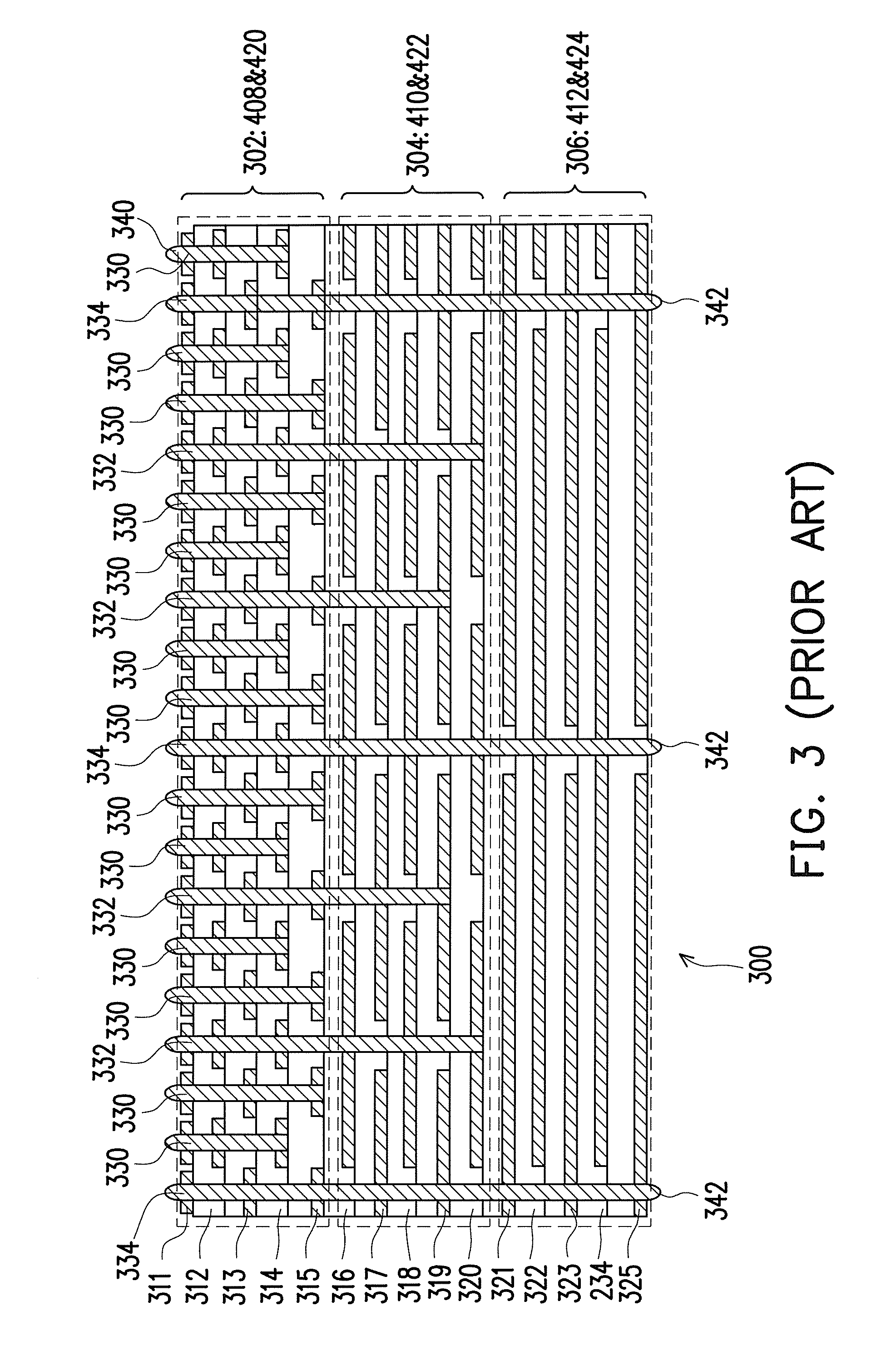
Accordingly, it suggests that assuming a number of conductive vias are disposed around a small capacitor structure (for example, 302 in FIG. 3), some of current-drawing points still may not contribute to reduce the expected effect of reducing inductance (since the conductive vias are not effectively connected in parallel).
Therefore, the inductor-capacitor combination scheme of FIG. 3 (a large capacitor paired with a large inductor, and a small capacitor paired with a small inductor) may not function as expected.
In other words, for the architecture of FIG. 3, only effectively parallel-connected conductive vias can effectively reduce the inductance; however, the architecture does not assure the conductive vias in effective parallel connection, which is a real obstacle to make the architecture function as a hierarchical decoupling capacitor structure.

Method used


Image

  • Stepwise capacitor structure, fabrication method thereof and substrate employing the same
  • Stepwise capacitor structure, fabrication method thereof and substrate employing the same
  • Stepwise capacitor structure, fabrication method thereof and substrate employing the same

Examples


Embodiment Construction

[0051]Reference will now be made in detail to the present preferred embodiments of the invention, examples of which are illustrated in the accompanying drawings. Wherever possible, the same reference numbers are used in the drawings and the description to refer to the same or like parts.

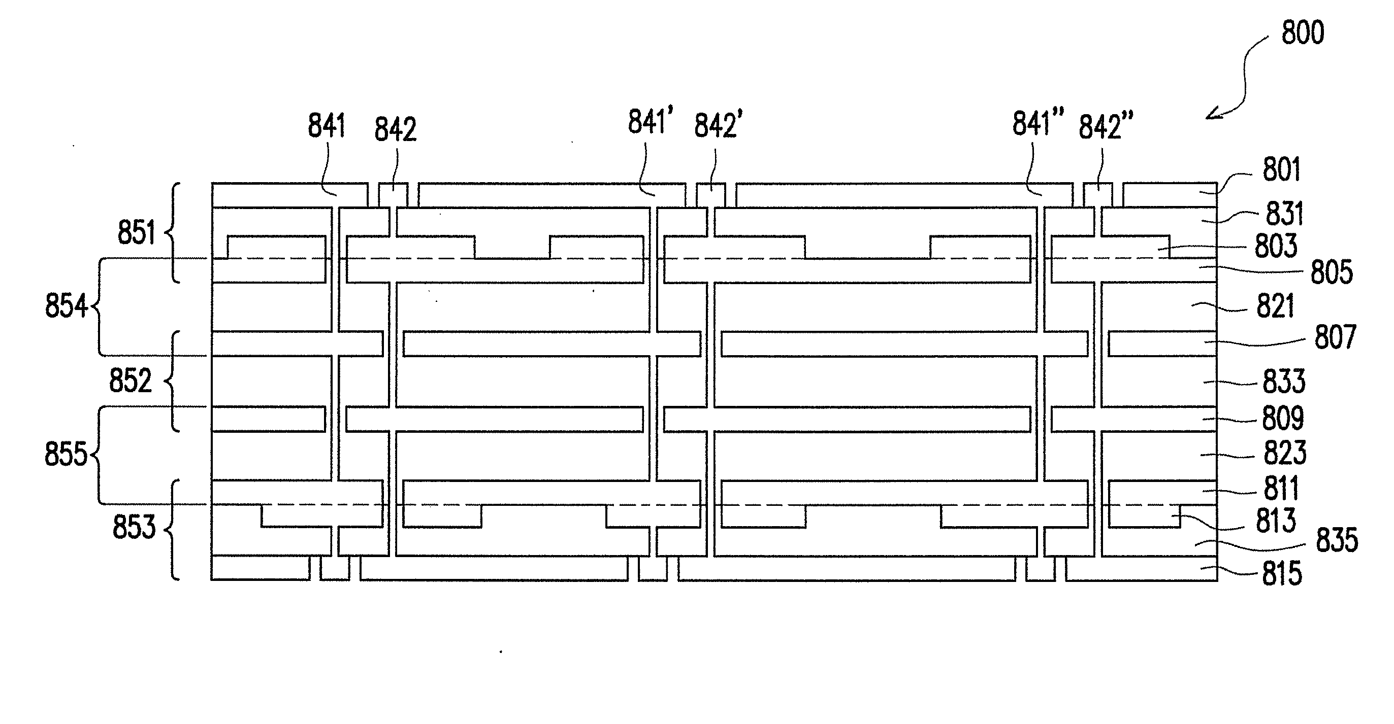
[0052]The present invention provides a stepwise capacitor structure and a substrate employing the stepwise capacitor structure, where current-drawing points of a die load may be paired with current paths having minimum impedance (i.e. minimum inductance) to achieve an effective parallel connection. In addition, the present invention also provides a method of fabricating a multi-layer stepwise capacitor structure capable of improving production yield and changing capacitance based on requirement.

[0053]In one embodiment, the present invention provides a stepwise capacitor structure and a substrate having the stepwise capacitor structure. In one embodiment, the stepwise capacitor structure includes a lo...


PUM


Abstract

A stepwise capacitor structure includes at least one stepwise conductive layer. The stepwise capacitor represents a feature of multiple capacitors. When currents flow through the stepwise capacitor, different current paths are presented in between an upper conductor and a bottom conductor of the stepwise capacitor in response to different current frequency; different inductor is induced in each path and decoupled by a stepwise capacitor structure as disclosed herein.

Description

CROSS-REFERENCE TO RELATED APPLICATION[0001]This is a continuation-in-part application of and claims the priority benefit of patent application Ser. No. 12 / 173,032, filed Jul. 15, 2008, now pending. The prior application Ser. No. 12 / 173,032 claims the priority benefit of Taiwan patent application Ser. No. 96144117, filed on Nov. 21, 2007. This application also claims the priority benefit of Taiwan application serial no. 97144950, filed Nov. 20, 2008. The entirety of each of the above-mentioned patent applications is hereby incorporated by reference herein and made a part of this specification.BACKGROUND OF THE INVENTION[0002]1. Field of the Invention[0003]The present invention relates to a capacitor structure, especially a stepwise capacitor structure which represents a feature of multiple capacitors; and a fabrication method thereof, and a substrate employing the same.[0004]2. Description of Related Art[0005]An electronic circuit today, such as a computer, has powerful functions an...

Claims


Application Information

Patent Timeline
IPC IPC(8): H01G4/30H01L21/34
CPCH01G4/012H01G4/232H01G4/30H01L23/50H01L2224/16225H01L28/40H01L2924/09701H01L2924/3011H01L23/642
Inventor LEE, MIN-LINWU, SHIH-HSIENLAI, SHINN-JUHLIU, SHUR-FEN
Owner IND TECH RES INST
Learn More