Method for producing display device

a display device and display technology, applied in the direction of solid-state devices, vacuum evaporation coatings, coatings, etc., can solve the problems of complex facilities, increased costs, inefficient and unrealistic, etc., and achieve excellent display characteristics

Inactive Publication Date: 2009-07-16
SONY CORP
View PDF8 Cites 37 Cited by
  • Summary
  • Abstract
  • Description
  • Claims
  • Application Information

AI Technical Summary

Benefits of technology

[0010]However, the foregoing operation needs additional large-scale equipment to rotate the substrate 5 and the deposition mask 3 through 90° in front and behind the vacuum chamber. Such additional equipment further needs means for moving the substrate 5 and the deposition mask 3 in directions parallel to their long and short sides. This results in complex facilities and increased costs.
[0011]In the case where the vapor deposition apparatus is so designed as to move the substrate 5 and the deposition mask 3 in the direction parallel to their short sides, moving them in the direction parallel to their long sides wastes the deposition material. By contrast, in the case where the vapor deposition apparatus is so designed as to move the substrate 5 and the deposition mask 3 in the direction parallel to their long sides, moving them in the direction parallel to their short sides causes variation in the thickness of deposited film on the substrate. This lowers yields.
[0013]Embodiments of the present invention were completed to address the foregoing problems. It is an aim of the embodiments of the present invention to provide a method for producing high-performance display devices economically without expanding the existing apparatus with additional equipment. The method permits reasonable arrangement of display panels on a substrate and also permits vapor deposition for sufficient film thickness over the broad effective pixel region.
[0016]The embodiments of the present invention permit pixels arranged in each display panel region to be covered with sufficiently thick deposit film over the broad effective pixel region while allowing the display panel regions to be arranged reasonably within the substrate without the necessity of modifying the existing deposition apparatus with additional equipment. Thus, it permits one to produce economically display devices excellent in display characteristics.

Problems solved by technology

This results in complex facilities and increased costs.
However, this is inefficient and unrealistic because the number of substrates to be supplied to the vapor deposition units depends on upstream steps.

Method used


Image

  • Method for producing display device
  • Method for producing display device
  • Method for producing display device

Examples


Embodiment Construction

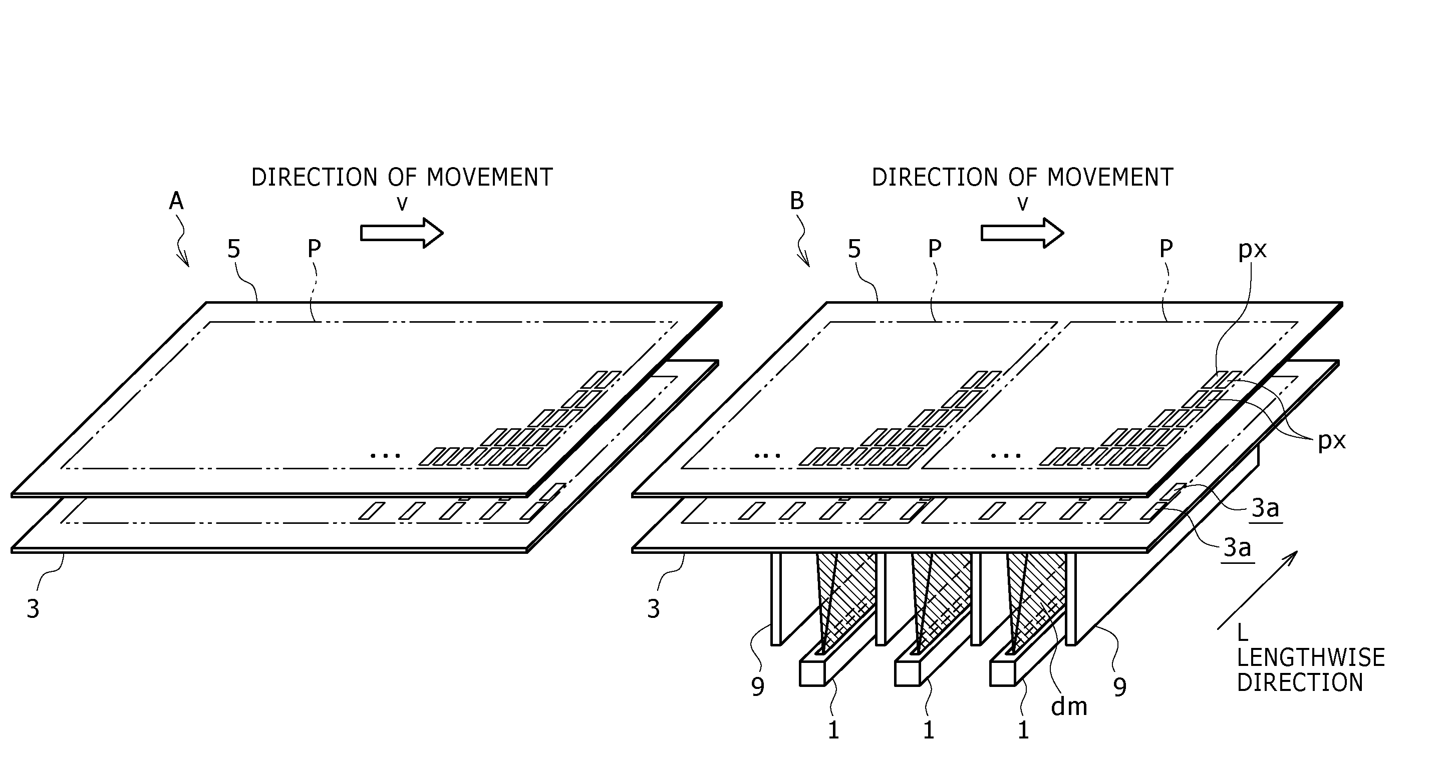
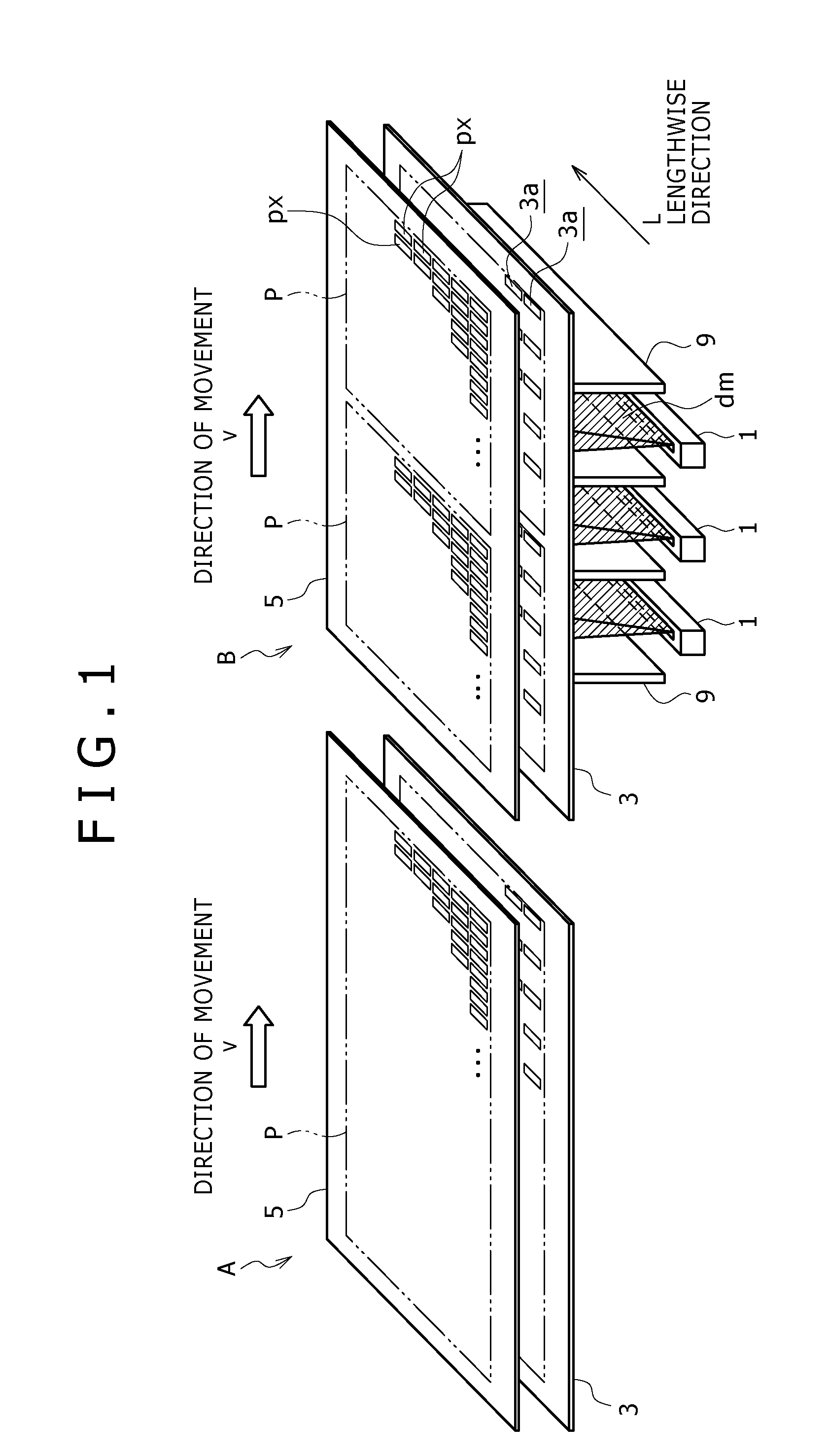
[0030]The embodiments of the present invention will be described with reference to the accompanying drawings. It is concerned with the production of an organic EL (electroluminescence) display device in which individual RGB pixels have respective organic EL elements. In this embodiment, the method according to the present invention is used to form the organic EL layer by vapor deposition. Incidentally, constituents identical with those in the existing technology are given the same symbols for explanation.

[0031]The display device is produced by using the vapor deposition apparatus having a plurality of elongated evaporation sources 1 arranged in parallel to one another, as shown in FIG. 1. Each evaporation source 1 has a length conforming to the size of the substrate 5 to be treated for vapor deposition. For example, the length may correspond to the short side (or long side) of the rectangular substrate 5. In other words, the length of the evaporation source 1 practically determines ...


PUM

PropertyMeasurementUnit
electroluminescenceaaaaaaaaaa
angle of evaporationaaaaaaaaaa
thicknessaaaaaaaaaa

Abstract

Disclosed herein is a method for producing display devices for forming deposited patterns conforming to pixels on a substrate by means of elongated evaporation sources and a deposition mask having regularly arranged apertures, the method including the steps of arranging the deposition mask and the substrate in such a way that the long sides of the apertures and pixels are parallel to the lengthwise direction of the evaporation sources irrespective of the direction in which the display panel regions are arranged within the substrate; and moving the substrate and the deposition mask relative to the evaporation sources, thereby forming the deposited patterns conforming to the pixels on the substrate.

Description

CROSS REFERENCES TO RELATED APPLICATIONS[0001]The present invention contains subject matter related to Japanese Patent Application JP 2008-005419 filed in the Japan Patent Office on Jan. 15, 2008, the entire contents of which being incorporated herein by reference.BACKGROUND OF THE INVENTION[0002]1. Field of the Invention[0003]The present invention relates to a method for producing display devices, which includes a step of forming a patterned film by vapor deposition through a mask corresponding to a plurality of pixels arranged in an array of columns and rows.[0004]2. Description of the Related Art[0005]The display device having organic electroluminescence elements arranged and formed therein is usually produced by vapor deposition, which permits organic light-emitting materials corresponding to RGB colors to be deposited on a substrate through a metal mask having a plurality of apertures corresponding to pixels.[0006]An example of mask vapor deposition is shown in FIG. 9 (perspect...

Claims


Application Information

Patent Timeline
Patent Type & Authority Applications(United States)
IPC IPC(8): B05D5/06
CPCC23C14/042H01L51/56H01L51/001C23C14/12H10K71/164H10K71/00
Inventor UETAKE, NAOKI
Owner SONY CORP
Why Eureka
Try Eureka