Driving configuration of a switch

a technology of driving configuration and switch, which is applied in the direction of pulse generators, electrical devices, transistors, etc., can solve problems such as serious drawbacks

Active Publication Date: 2009-07-23
STMICROELECTRONICS SRL
View PDF5 Cites 12 Cited by
  • Summary
  • Abstract
  • Description
  • Claims
  • Application Information

AI Technical Summary

Benefits of technology

[0021]The technical problem is that of providing a driving configuration of a high voltage switch able to associate, with a quick switch transient, a reasonable control current value while overcoming the limits and drawbacks still affecting the configurations realized according to the foregoing description.

Problems solved by technology

Although advantageous under several aspects, this known configuration shows a serious drawback linked to the sizing of the resistive element Rgs inserted between the common gate GG and the source SS terminals of the DM1 and DM2 transistors of the switch 1.
The technical problem is that of providing a driving configuration of a high voltage switch able to associate, with a quick switch transient, a reasonable control current value while overcoming the limits and drawbacks still affecting the configurations realized according to the foregoing description.

Method used


Image

  • Driving configuration of a switch
  • Driving configuration of a switch
  • Driving configuration of a switch

Examples


Embodiment Construction

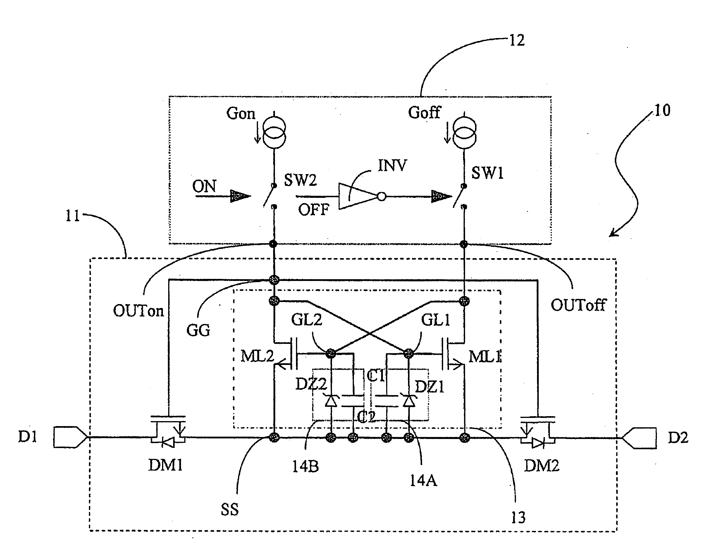
[0068]With reference to these figures, and in particular to FIG. 3, a driving configuration of a switch 10, in particular a high voltage switch driven by a driving device or driver is globally and schematically illustrated.

[0069]Elements structurally and functionally corresponding to the driving configuration described in relation to FIG. 1 will be given the same reference numbers by way of illustration.

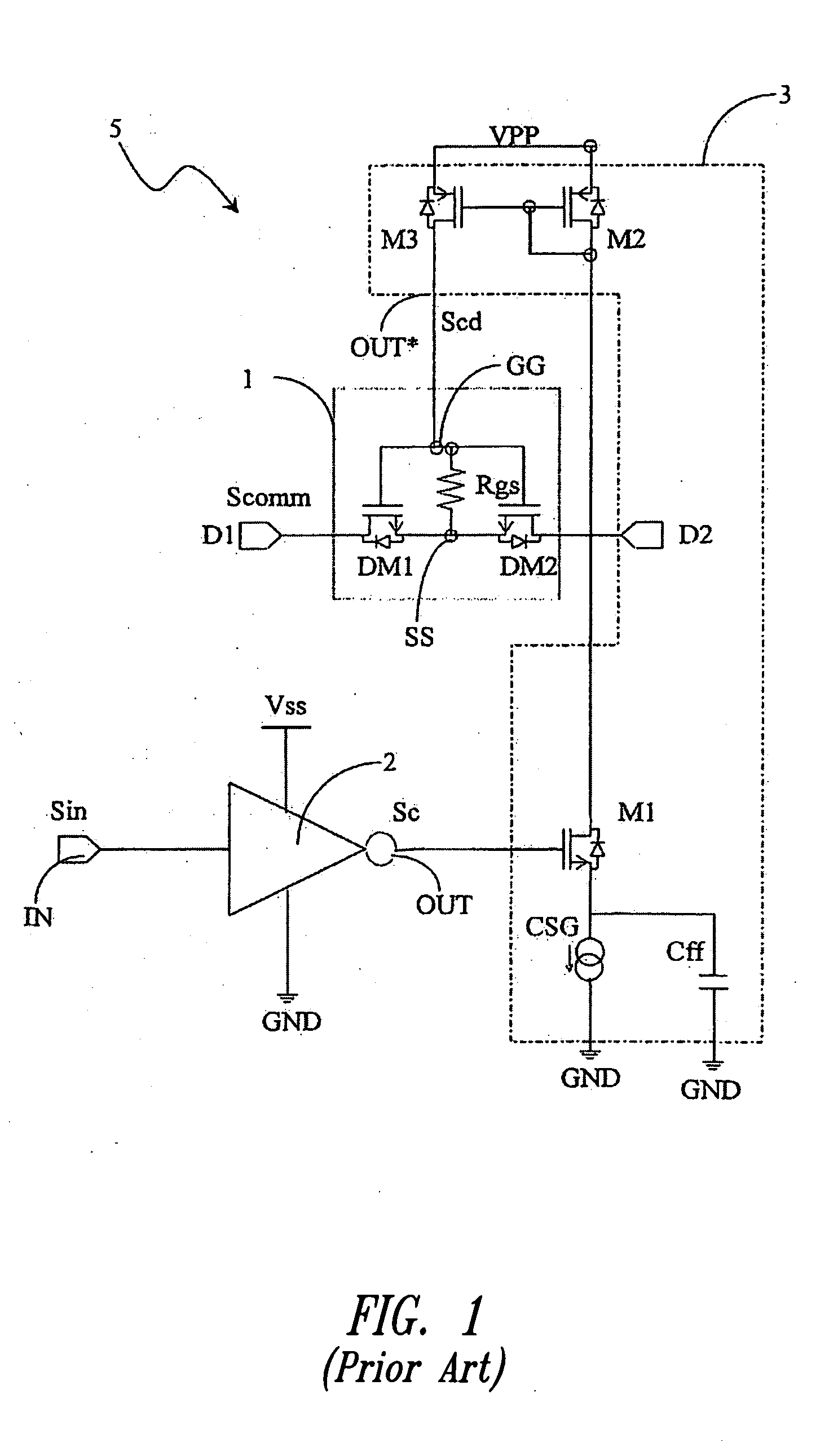
[0070]In particular, the driving configuration 10 includes a switch 11 realized by means of first and second transistors, DM1 and DM2, in particular MOS or DMOS transistors, connected, in series to each other and to relative intrinsic diodes in antiseries, i.e., to a pair of corresponding terminals, in particular anodes, in common.

[0071]The switch 11 is driven by a driving device or driver 12 having first OUT“off” and second OUT“on” output terminals connected to the switch 11.

[0072]The driver 12 essentially includes first Goff and second Gon control current generators connected, by m...


PUM


Abstract

A driving circuit of a switch includes first and second transistors connected in series to each other and to relative intrinsic diodes in antiseries and driven by a driving device that includes at least one first and one second output terminal connected to the switch to supply it with a first control signal for driving the switch in a first working state and a second control signal for driving the switch in a second working state. At least one latch circuit coupled between respective common gate and source terminals of the first and second transistors supplies the common gate terminal with the first and second control signals, respectively, according to the working state to turn off and turn on the first and second transistors. The latch circuit comprises at least one flip-flop coupled to the common source terminal and having a reset terminal coupled to the first output terminal of the driving device and to the common source terminal by means of a reset resistance, a set terminal coupled to the second output terminal of the driving device and to the common source terminal by means of a set resistance and an output terminal coupled to the common gate terminal. The latch circuit further includes an activation circuit connected to the set and reset terminals of the flip-flop and to the common source terminal in order to dynamically short-circuit the set and reset resistances during the falling edges of the signal applied to the switch.

Description

BACKGROUNDRelated Application[0001]The present application is a Continuation-In-Part of the U.S. patent application Ser. No. 11 / 753,839 filed on May 25, 2007, the disclosure of which is incorporated herein by reference.Technical Field[0002]The present disclosure relates to the driving configuration of a switch and, more specifically, to a driving configuration of a switch realized by means of a first and a second transistor connected in series to each other and to the relative intrinsic diodes in antiseries and driven by a driving device, including, without limitation, a driving configuration of a high voltage (HV) switch.Description of the Related Art[0003]As is well known, a driving device of a high voltage (HV) switch, usually realized by means of a MOS transistor, is specified to instantaneously follow the voltage dynamics of a signal to be switched.[0004]In general, a switch realized by means of a high voltage MOD or DMOS transistor is able to manage high voltages between its d...

Claims


Application Information

Patent Timeline
Patent Type & Authority Applications(United States)
IPC IPC(8): H03K3/00H03K17/56H03K17/687
CPCH03K17/6874H03K17/04206
Inventor RICOTTI, GIULIODEPETRO, RICCARDO
Owner STMICROELECTRONICS SRL
Why Eureka
Try Eureka