
Semiconductor memory device

a memory device and semiconductor technology, applied in the direction of information storage, static storage, digital storage, etc., can solve the problems of excessive data preservation margin, restricted standby current consumption, and associated standby current consumption

Active Publication Date: 2011-12-27
DENSO CORP
View PDF15 Cites 14 Cited by
  • Summary
  • Abstract
  • Description
  • Claims
  • Application Information

AI Technical Summary

Benefits of technology

[0008]The various inventive embodiments described in the present application address the above described and other situations, and provide a semiconductor memory device capable of ensuring a margin for data preservation while suppressing a current consumption required when, for example, a low-power consumption mode is designated.
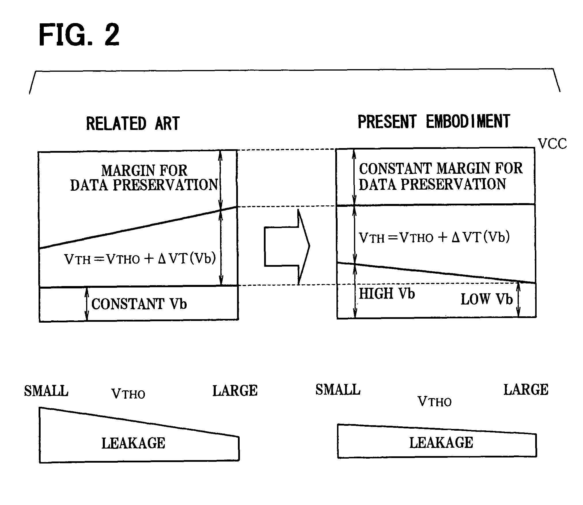
[0009]According to one aspect, each of static random-access memory (SRAM) cells includes memory cell transistors. A regulation circuit regulates a voltage applied to the sources or the back gates of the memory cell transistors so that even when the threshold voltage of the memory cell transistors included in each of the SRAM cell fluctuates, a margin for turning on of the memory cell transistors can always be retained at a certain value. While a standby current consumption is suppressed by reducing leakage currents of the memory cell transistors due to an effect of a bias voltage applied to a substrate, a stable margin for data preservation can be ensured.
[0010]In accordance with another aspect, each of SRAM cells includes memory cell transistors. Each of detection circuits detects the threshold voltage of the memory cell transistors. A regulation circuit regulates a voltage applied to the sources or the back gates of the memory cell transistors, on the basis of the result of the detection performed by each of the detection circuits. The value of the margin for data preservation can therefore be controlled.

Problems solved by technology

Since the effect of a bias voltage applied to a substrate is limited, if the threshold voltage Vt is decreased due to a variance caused by high temperature or a manufacturing process, a margin for data preservation becomes excessively large, however, a reduction in a standby current consumption is restricted.
A standby current consumption associated, for example, with a low-power consumption mode tends to pose a problem because of an off-leakage current of a metal-oxide semiconductor (MOS) transistor.

Method used


Image

  • Semiconductor memory device
  • Semiconductor memory device
  • Semiconductor memory device

Examples


first embodiment

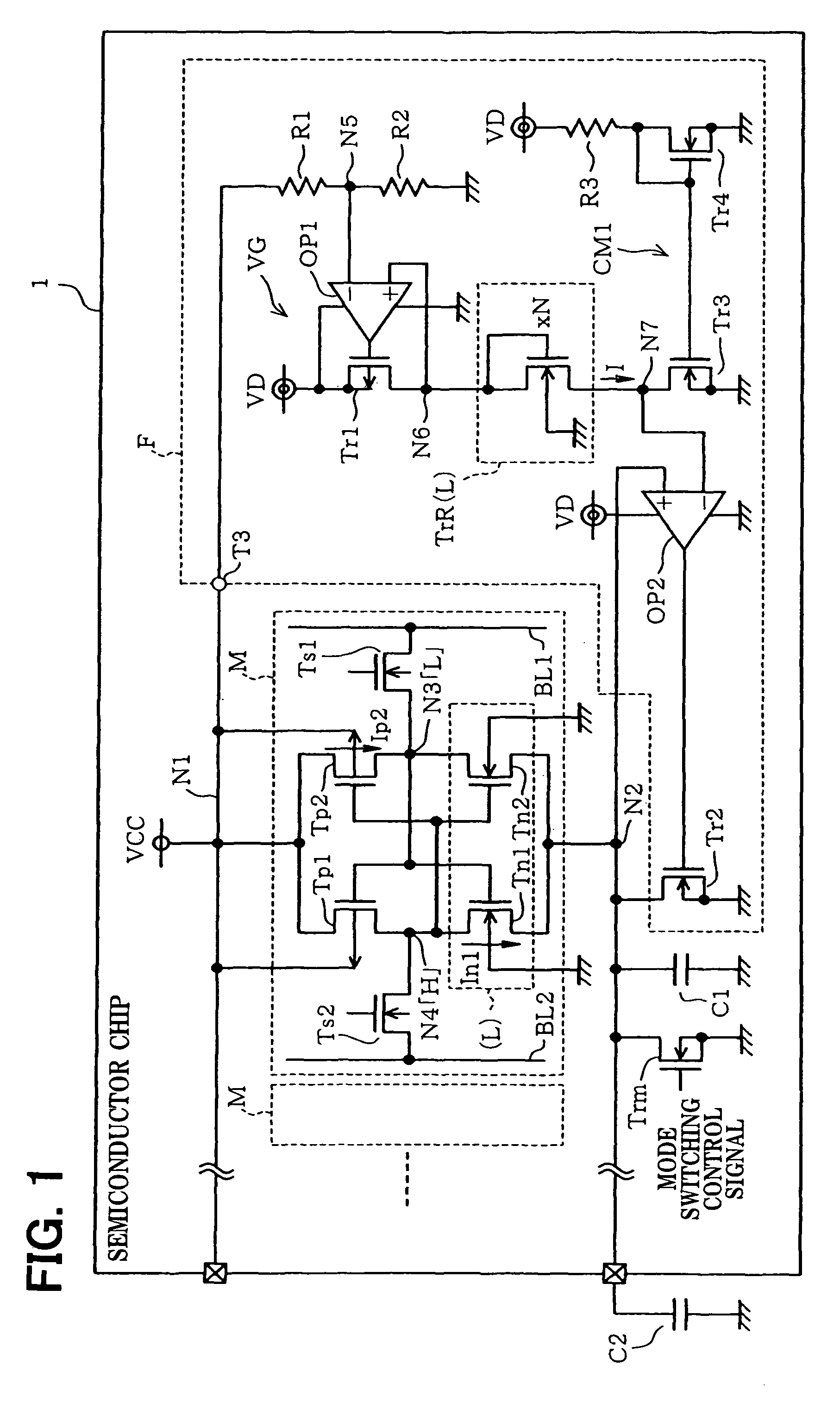
[0030]Referring to FIG. 1 and FIG. 2, a first embodiment involves a semiconductor memory device that employs a static random access memory (SRAM) cell as will be described below.

[0031]FIG. 1 is a circuit diagram showing the electrical constitution of a fully complementary metal-oxide semiconductor (CMOS) type SRAM and a regulation circuit that regulates a source potential. The semiconductor memory device is included in a system that may be mounted in a vehicle and that operates while being externally powered with a predetermined voltage such as, for example, 5 V.

[0032]An exemplary semiconductor memory device may be embodied as semiconductor chip 1. Numerous memory cells M are formed as a matrix on, for example, a thin-film silicon-on-insulator (SOI) substrate (not shown). FIG. 1 shows one of the memory cells M. The memory cell M preserves data when having a memory cell supply voltage VCC of, for example, 1.2 V applied thereto. The memory cell M includes an inverter pair including a ...

second embodiment

[0064]FIG. 3 shows a second embodiment. The same reference numerals are assigned to components identical to those of a first embodiment. A redundant description will be omitted, and a difference will be described below.

[0065]As shown in FIG. 3, a regulation circuit F2 is formed in a semiconductor chip 11, which, for example for comparison purposes, corresponds to the semiconductor chip 1 and the regulation circuit F described herein above. The regulation circuit F2 has an electrical constitution described below in addition to the electrical constitution of the regulation circuit F. An n-channel MOS transistor Tr5 is formed in place of the resistor R2. The drain of the MOS transistor Tr5 is connected to the resistor R1, and the source thereof is connected to a ground. A resistor R4 and the drain and source of an n-channel MOS transistor Tr6 are connected in series with one another between the node N1 and ground.

[0066]Resistors R5 and R6 for voltage division are also connected in seri...

third embodiment

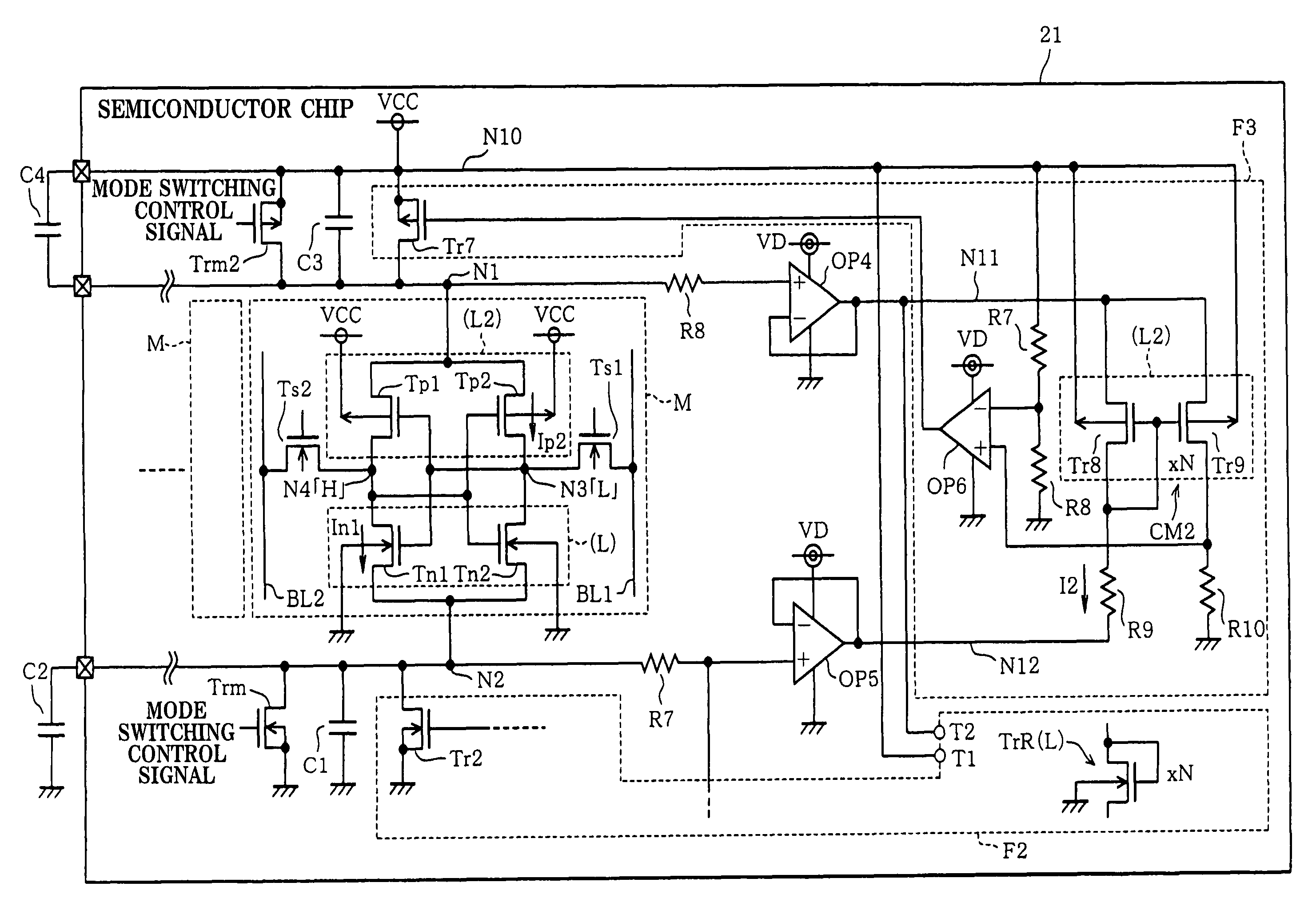
[0070]FIG. 4 to FIG. 5B show a third embodiment. A difference from the above described embodiments is that a bias voltage is applied to the node connected to the sources of the n-channel MOS transistors and also to the node connected to the sources of the p-channel MOS transistors included in each of the memory cells. Thus, a third embodiment is intended to exert an effect of reduction of leakage currents.

[0071]FIG. 4 shows a semiconductor chip 21, which, for example for comparison purposes, corresponds to the semiconductor chips 1 and 11. The regulation circuit F2 described in relation to the above described embodiment is formed in the semiconductor chip 21, and designed to apply a voltage to the node N2. In the above described embodiments, a connecting terminal T1 via which power is fed to the resistors R5 and R6 and a connecting terminal T2 via which power is fed to the resistor R1 are connected to the power feeding node N1 through which a supply voltage VCC is fed. In the presen...


PUM


Abstract

In a memory cell, a margin for data preservation is provided while suppressing a current consumption associated with a low-power consumption mode. A MOS transistor has the same structure as NMOS transistors included in each of memory cells. When a low-power consumption mode is designated, a voltage developed at a node is stabilized by subtracting a margin voltage for data preservation across a first resistor from a voltage applied to a first node and by subtracting a threshold voltage of the MOS transistor from the resultant voltage is applied to a second node.

Description

CROSS REFERENCE TO RELATED APPLICATIONS[0001]The present application is based on and claims priority to Japanese Applications JP 2008-083798, filed on Mar. 27, 2008, and JP 2008-295502, filed on Nov. 19, 2008, the contents of which are incorporated herein by reference.BACKGROUND OF THE INVENTION[0002]1. Field of the Invention[0003]The present invention relates to a semiconductor memory device and, more specifically, for reducing current consumption and preserving stored data when a low-power consumption mode is designated.[0004]2. Description of the Related Art[0005]In the technological field of semiconductor memory devices, there is always a demand for low current consumptive devices. A technology has been developed, for example, as described in JP-A-2000-174611, in which a bias voltage is applied to the sources of memory transistors included in a memory cell in order to suppress a current consumption required by the memory device when a low-power consumption mode is designated. Th...

Claims


Application Information

Patent Timeline
Patent Type & Authority Patents(United States)
IPC IPC(8): G11C11/00
CPCG11C11/413
Inventor INOUE, AKIMITSU
Owner DENSO CORP
Learn More