Contact hole forming method of semiconductor component

A contact hole and semiconductor technology, which is applied in semiconductor devices, semiconductor/solid-state device manufacturing, electrical components, etc., can solve the problems of deformation and deterioration of semiconductor components

Inactive Publication Date: 2006-08-16
KEY FOUNDRY CO LTD
View PDF0 Cites 0 Cited by
  • Summary
  • Abstract
  • Description
  • Claims
  • Application Information

AI Technical Summary

Problems solved by technology

[0028] Another object of the present invention is to provide a method for forming a contact hole in a semiconductor element, wherein a silicon nitride layer is preliminarily formed on the active area to solve the problem due to the silicon surface lattice (lattice) structure in the active area. Deterioration of semiconductor device characteristics caused by ion implantation deformation

Method used


Image

  • Contact hole forming method of semiconductor component
  • Contact hole forming method of semiconductor component
  • Contact hole forming method of semiconductor component

Examples


Embodiment Construction

[0070] Below, describe preferred specific embodiment of the present invention in detail with reference to accompanying drawing, in following description and accompanying drawing, with identical reference number designate identical or similar component, and for identical or similar component, its repeated description will give omitted.

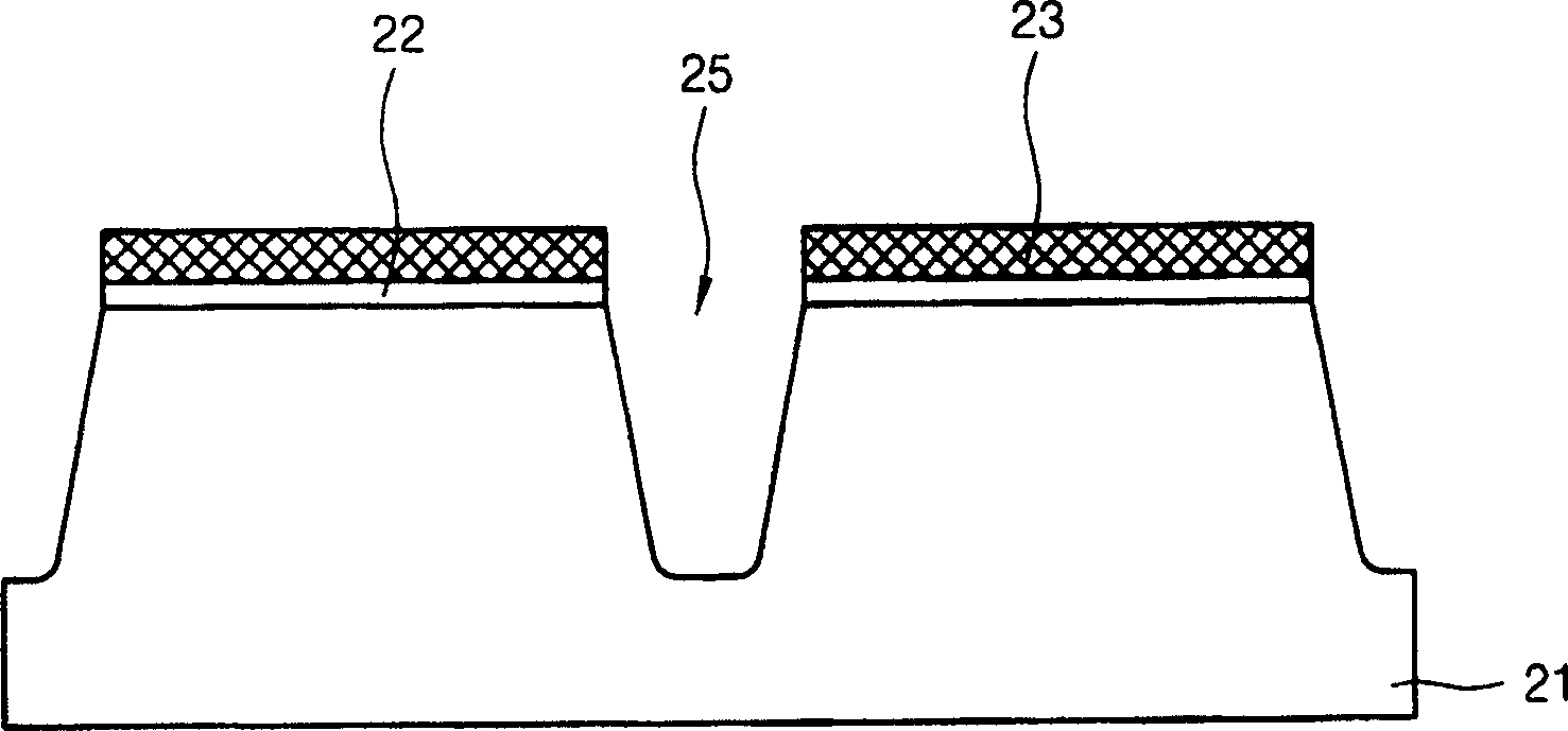
[0071] Figures 3A to 3I is a cross-sectional view illustrating a method of forming a contact hole in a semiconductor package according to the present invention.

[0072] see Figure 3A , depositing a pad oxide layer (SiO 2 ) layer 102, and then deposit a predetermined thickness of silicon nitride (Si 3 N 4 ) 104, at this time, the deposited silicon nitride layer (Si 3 N 4 ) 104 fills the interior of the trench with deposited oxide in a subsequent step and serves as a polishing stop layer when planarized using a chemical mechanical polishing (CMP) process;

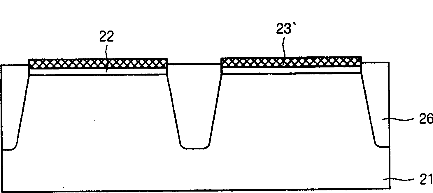
[0073] Secondly, after coating the photosensitive material 106 on the silicon ni...


PUM


Abstract

Disclosed is a method for forming a contact hole in the process of manufacturing a logic device employing a shallow trench isolation (STI) method. The method prevents an isolation region from being damaged because there is little overlap margin for a contact hole in the active region, when a contact hole is formed in an isolation region beyond the border of an active region, that is, when a borderless contact hole is formed. According to the method, a silicon nitride layer used as an etch-stop layer is formed in the process of providing the STI, thereby avoiding deterioration of the characteristics of a resulting semiconductor device.

Description

technical field [0001] The present invention relates to a method for forming a contact hole of a semiconductor element, and in particular relates to making the overlapping distance (Overlap Margin) of the contact hole smaller in the active region, and the contact hole can be formed between the active region (active region) and the isolation region ( isolation region) at the same time; that is, when forming a borderless contact hole, it is a method of forming a contact hole of a semiconductor element that can prevent damage to the isolation region. Background technique [0002] In terms of the design and structure of the logic device, it is necessary to form the contact hole only on the control electrode (gate) or the active region (Active Region). However, to reduce the size of the logic components, the overlap margin of the contact holes facing the active area is also reduced. As a result, misalignment occurs in the lithography process. , a part of the contact hole that mu...

Claims


Application Information

Patent Timeline
IPC IPC(8): H01L21/30H01L21/3065H01L21/28H01L21/60H01L21/762H01L21/8234
CPCH01L21/823481H01L21/76224H01L21/823475H01L21/76897H01L21/28
Inventor 朴根周
Owner KEY FOUNDRY CO LTD
Why Eureka
Try Eureka