Phase change memory device with alternating adjacent conduction contacts and fabrication method thereof

a phase change memory and conduction contact technology, applied in semiconductor devices, digital storage, instruments, etc., can solve the problems of reducing the yield of the device, and difficult to ensure the desired cd

Active Publication Date: 2010-12-02
SK HYNIX INC
View PDF1 Cites 0 Cited by
  • Summary
  • Abstract
  • Description
  • Claims
  • Application Information

AI Technical Summary

Benefits of technology

[0013]The inventive concept provides a phase change memory device and a method for manufacturing the same being capable of ensuring the margin between adjacent word line contacts.

Problems solved by technology

Accordingly, it is difficult to ensure the desired CD (Critical Dimension) in patterning holes for the word line contacts 121.
Furthermore, since the space between the patterns becomes narrower, then a bridge with the adjacent holes can occur and thereby reduces the yield of the device.
As the level of integration increases for semiconductor memory devices, it is becoming more difficult to ensure the desired CD.
Furthermore, it becomes more and more difficult to ensure the minimum requirements to prevent misalignments as a result of downsizing the dimensional layout ratios of the device.
Furthermore, when the diameter in the contact hole is reduced based on the demands for more highly integrated devices, then gap filling is more likely to be degraded which reduces the productivity of device.

Method used


Image

  • Phase change memory device with alternating adjacent conduction contacts and fabrication method thereof
  • Phase change memory device with alternating adjacent conduction contacts and fabrication method thereof
  • Phase change memory device with alternating adjacent conduction contacts and fabrication method thereof

Examples


Embodiment Construction

.”

BRIEF DESCRIPTION OF THE DRAWINGS

[0019]The above and other aspects, features and other advantages of the subject matter of the present disclosure will be more clearly understood from the following detailed description taken in conjunction with the accompanying drawings, in which:

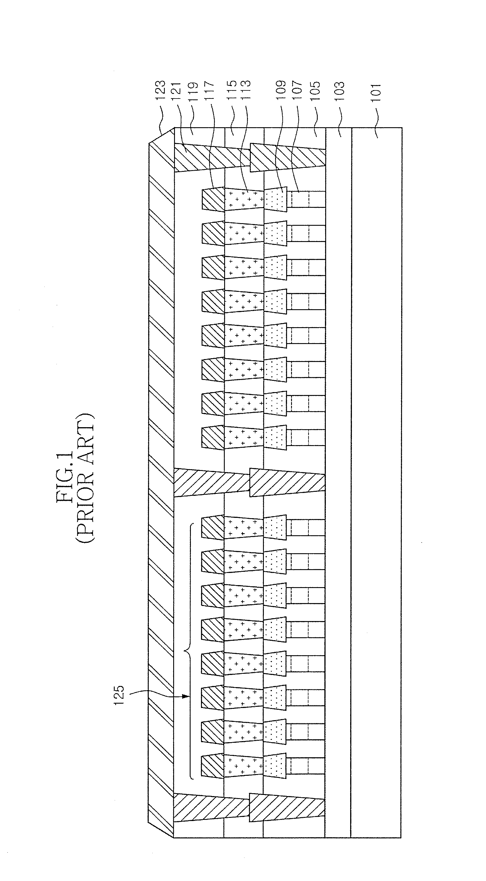
[0020]FIG. 1 is a sectional view of a conventional phase change memory device;

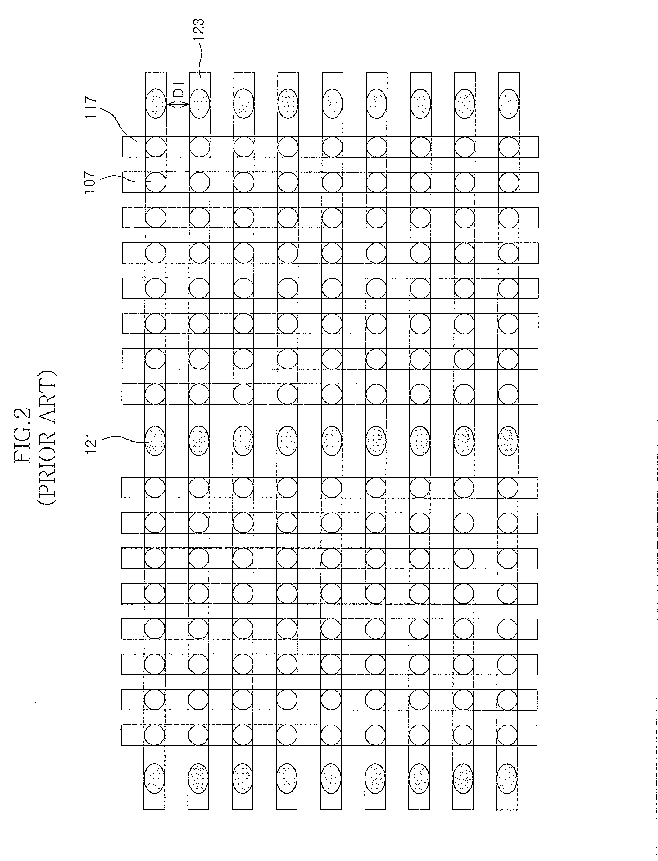
[0021]FIG. 2 is a lay out of the conventional phase change memory device in FIG. 1;

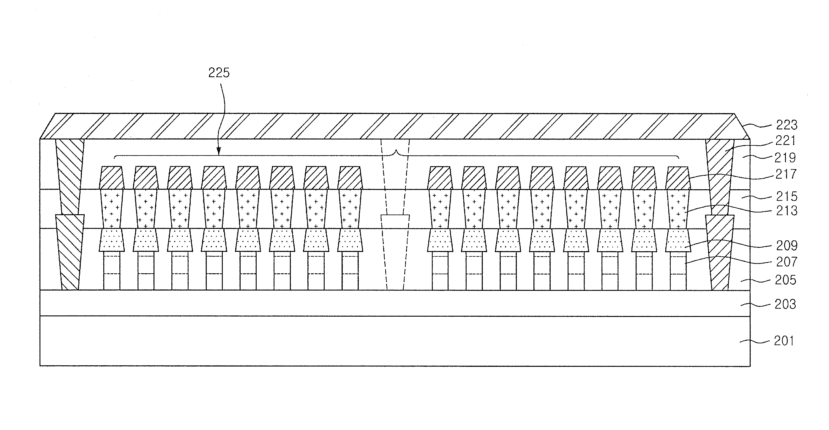
[0022]FIG. 3 is a lay out of a phase change memory device according to an example embodiment;

[0023]FIG. 4 is a sectional view of the phase change memory device in FIG. 3; and

[0024]FIG. 5 is a lay out of a phase change memory device according to another example embodiment.

DETAILED DESCRIPTION

[0025]Exemplary embodiments are described herein with reference to cross-sectional illustrations that are schematic illustrations of exemplary embodiments (and intermediate structures). As such, variations from the shapes of the illustrations as a result, for ex...


PUM


Abstract

A phase change memory device and an associated method of making same are presented. The phase change memory device, includes first wiring lines, second wiring lines, memory cells, and conduction contacts. The first wiring lines are arranged substantially in parallel to each other so that the first wiring lines are grouped into odd and even numbered first wiring lines. The memory cells are coupled to the first and second wiring lines. The conduction contacts coupled to the first wiring lines so that only one conduction contact is coupled to a center of a corresponding odd numbered first wiring line. Also only two corresponding conduction contacts are coupled to opposing edges of a corresponding even numbered first wiring line. Accordingly, the conduction contacts are arranged on the first wiring lines so that conduction contacts are not adjacent to each other with respect to immediately adjacent first wiring lines.

Description

CROSS-REFERENCES TO RELATED APPLICATION[0001]The present application claims priority under 35 U.S.C. 119(a) to Korean application number 10-2009-0048357, filed on Jun. 2, 2009, in the Korean Patent Office, which is incorporated by reference in its entirety as if set forth in full.BACKGROUND[0002]1. Technical Field[0003]The embodiments described herein relate to a semiconductor memory device and, more particularly, to a phase-change memory device and a method for manufacturing the same.[0004]2. Related Art[0005]A phase change random access memory (PRAM) is regarded as a non-volatile memory device. PRAMs are manufactured using a phase-change material which is capable of reversibly changing phases between an ordered crystalline solid state phase and a disordered amorphous solid state phase as a function of temperature. PRAMs also provide a way of storing a set status or a reset status because their different solid state phases exhibit distinctly different resistance difference.[0006]PR...

Claims


Application Information

Patent Timeline
Patent Type & Authority Applications(United States)
IPC IPC(8): H01L45/00H01L21/768H01L27/04
CPCG11C13/0004H01L27/2409H01L45/1233H01L45/06H01L27/2463H10B63/20H10B63/80H10N70/231H10N70/826H10B12/48
Inventor LEE, JANG UKCHOI, KANG SIK
Owner SK HYNIX INC
Why Eureka
Try Eureka