Non-volatile memory with single floating gate and method for operating the same

Inactive Publication Date: 2009-07-23
YIELD MICROELECTRONICS CORP
View PDF6 Cites 4 Cited by
  • Summary
  • Abstract
  • Description
  • Claims
  • Application Information

AI Technical Summary

Benefits of technology

[0005]An object of the present invention is to provide a non-volatile memory with single floating gate and the method for operating the same, which only require

Problems solved by technology

Data in volatile memories can only be kept through continual supply of power.
In this

Method used


Image

  • Non-volatile memory with single floating gate and method for operating the same
  • Non-volatile memory with single floating gate and method for operating the same
  • Non-volatile memory with single floating gate and method for operating the same

Examples


first embodiment

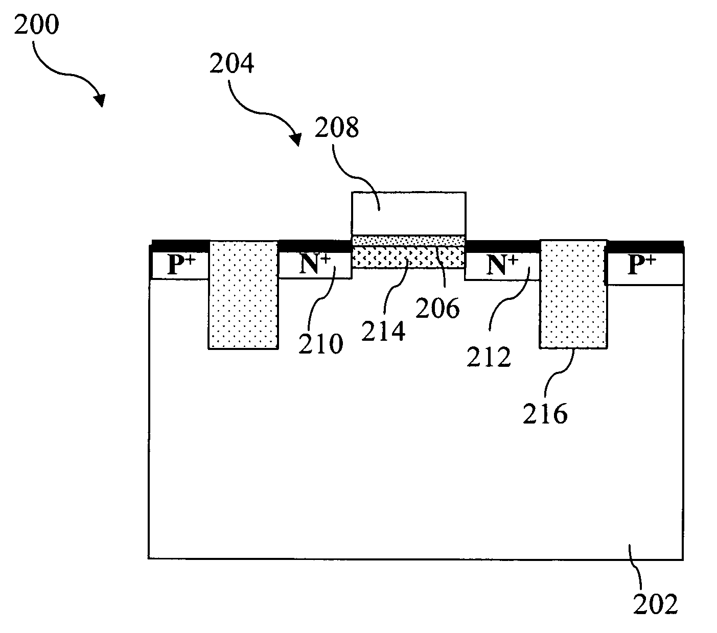
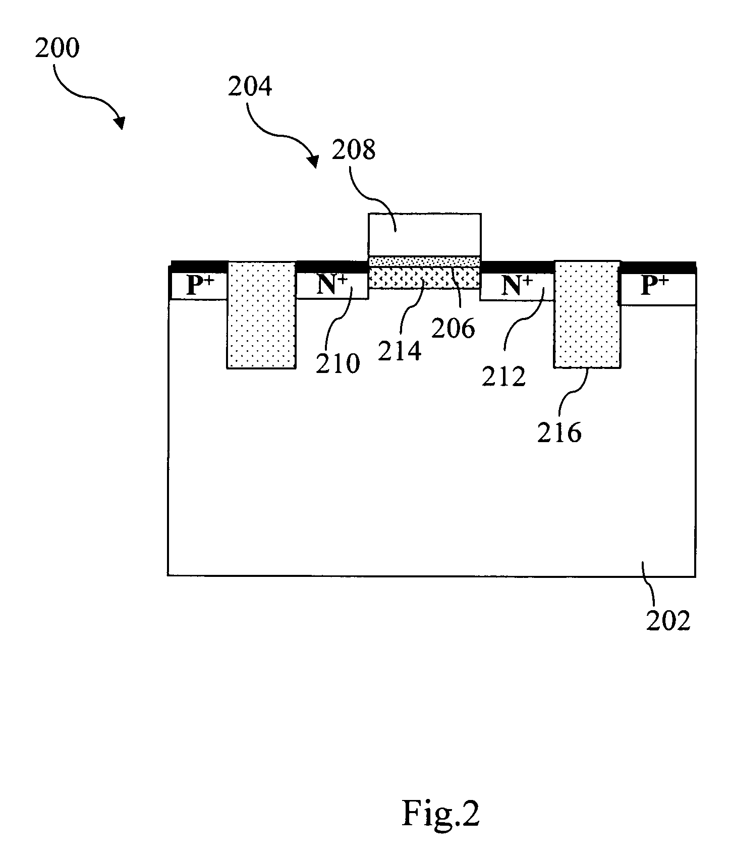
[0023]FIG. 2 is a cross-sectional view of the structure of a non-volatile memory with single floating gate according to the present invention. As shown in FIG. 2, a non-volatile memory with single floating gate 200 comprises a p-type semiconductor substrate 202, and at least an NMOS field-effect FET (NMOSFET) 204 located on the p-type semiconductor substrate 202.

[0024]The NMOSFET 204 includes a dielectric 206 located on the surface of the p-type semiconductor substrate 202, a floating gate 208 disposed on the dielectric 206, two n-type ion-doped regions respectively disposed in the p-type semiconductor substrate 202 at two sides of the dielectric 206 and used as a source 210 and a drain 212, and a channel 214 located in the p-type semiconductor substrate 202 between the source 210 and the drain 212.

[0025]This non-volatile memory with single floating gate is a structure having three terminals. As shown in FIG. 3, these three terminals respectively connect to the source 210, the drain...

second embodiment

[0039]FIG. 4 is a cross-sectional view of the structure of a non-volatile memory with single floating gate according to the present invention. As shown in FIG. 4, a non-volatile memory with single floating gate 300 comprises an n-type semiconductor substrate 302, a p-well 304 located in the n-type semiconductor substrate 302, and at least an NMOSFET 306 located on the p-well 304.

[0040]The NMOSFET 306 includes a dielectric 308 located on the surface of the p-well 304, a floating gate 310 disposed on the dielectric 308, two n-type ion-doped regions respectively disposed in the p-well 304 at two sides of the dielectric 308 and used as a source 312 and a drain 314, and a channel 316 located in the p-well 304 between the source 312 and the drain 314.

[0041]A substrate voltage Vsub, a p-well voltage Vp-well, a source voltage Vs, and a drain voltage Vd are respectively applied to the n-type semiconductor substrate 302, the p-well 304, the source 312, and the drain 314. The low-voltage opera...


PUM


Abstract

A non-volatile memory with single floating gate and the method for operating the same are proposed. The non-volatile memory is formed by embedding a FET structure in a semiconductor substrate. The FET comprises a single floating gate, a dielectric, and two ion-doped regions in the semiconductor at two sides of the dielectric. The memory cell of the proposed nonvolatile memory with single floating gate can perform many times of operations such as write, erase and read by means of a reverse bias.

Description

FIELD OF THE INVENTION[0001]The present invention relates to a non-volatile memory with single floating gate capable of writing and erasing many times and the method for operating the same and, more particularly, to a non-volatile memory with single floating gate capable of writing and erasing many times without the need of any control gate and the method for operating the same.BACKGROUND OF THE INVENTION[0002]Memory devices can generally be classified into two categories: volatile memories and non-volatile memories. Data in volatile memories can only be kept through continual supply of power. On the contrary, data in non-volatile memories can be maintained for a very long time even if the power is cut off. Therefore, non-volatile memories have been widely used in electronic products.[0003]In a non-volatile memory with single floating gate, two field-effect transistors (FETs) or one FET and one capacitor are generally grouped together. For example, as shown in FIG. 1, a non-volatile...

Claims


Application Information

Patent Timeline
IPC IPC(8): G11C16/06H01L29/788
CPCG11C16/0416G11C2216/10H01L29/788H01L29/66825H01L27/11558H10B41/60
Inventor LIN, HSIN CHANGHUANG, WEN CHIENYANG, MING TSANG
Owner YIELD MICROELECTRONICS CORP
Why Eureka
Try Eureka