Semiconductor module

A technology for semiconductors and shells, which is applied in semiconductor devices, semiconductor/solid-state device manufacturing, semiconductor/solid-state device components, etc., can solve problems such as damage to moisture resistance and increase in the area of ​​packaging materials, so as to reduce the amount of intrusion and reduce water permeability performance, and the effect of improving moisture resistance

Pending Publication Date: 2021-07-23
MITSUBISHI ELECTRIC CORP
View PDF6 Cites 0 Cited by
  • Summary
  • Abstract
  • Description
  • Claims
  • Application Information

AI Technical Summary

Problems solved by technology

[0004] However, since both the injection port and the exhaust port need to be provided in the cover, there is a problem that the area exposed to the atmosphere of the sealing material increases and the moisture resistance is impaired.

Method used


Image

  • Semiconductor module
  • Semiconductor module
  • Semiconductor module

Examples


Embodiment approach 1

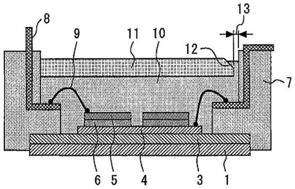
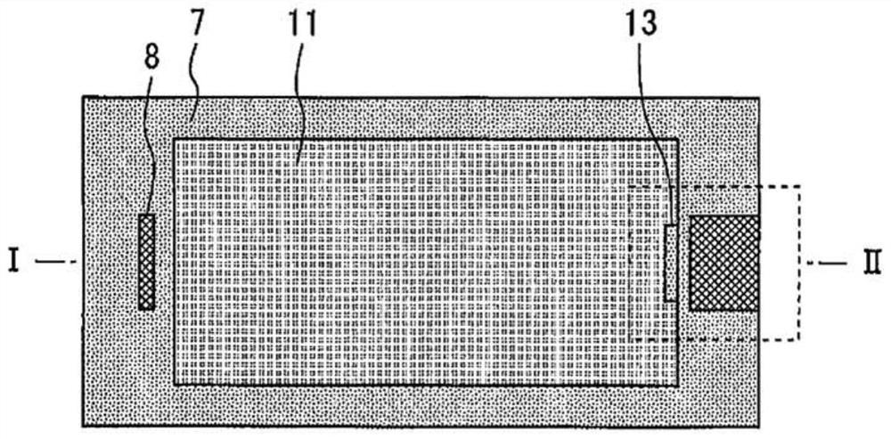
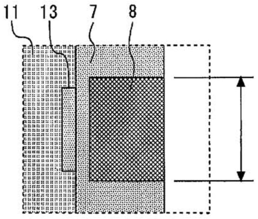
[0037] figure 1 It is a sectional view showing the semiconductor module according to the first embodiment. figure 2 It is a plan view showing the semiconductor module according to Embodiment 1. figure 1 is along figure 2 Sectional view of I-II. image 3 will be figure 2 A magnified top view of the portion enclosed by the dashed line.

[0038] An insulating layer 3 made of resin or ceramics is formed on the base plate 1 . A circuit pattern 4 is formed on the insulating layer 3 . The semiconductor chip 5 is mounted on the circuit pattern 4 via solder 6 . The semiconductor chip 5 is an IGBT chip or a diode chip. The case 7 is bonded to the outer peripheral portions of the base plate 1 and the insulating layer 3 so as to surround the circuit pattern 4 and the semiconductor chip 5 . The terminal electrodes 8 of the case 7 are connected to the upper surface electrodes of the semiconductor chip 5 through wires 9 .

[0039] A packaging material 10 such as silicone gel is i...

Embodiment approach 2

[0045] Figure 7 It is a sectional view showing the cover of the semiconductor module according to the second embodiment. Figure 8 It is a sectional view showing the semiconductor module according to the second embodiment. In the present embodiment, a tapered protrusion 14 whose central portion protrudes toward the sealing material 10 is provided on the lower surface of the cover 11 .

[0046] Figure 9 It is a cross-sectional view showing the manufacturing process of the semiconductor module according to the second embodiment. Even if air bubbles are formed at the interface between the packaging material 10 and the cover 11 when the cover 11 is placed on the upper surface of the packaging material 10, the air bubbles will be squeezed out along the tapered portion of the protrusion 14, from the casing 7 and the cover 11. The gap 13 in between is drained. As a result, the function of discharging air bubbles is higher than that of the first embodiment. Furthermore, the area ...

Embodiment approach 3

[0048] Figure 10 It is a perspective view showing the lower surface side of the cover of the semiconductor module according to the third embodiment. Figure 11 It is a plan view showing the cover of the semiconductor module according to the third embodiment. Figure 12 is along Figure 11 Sectional view of I-II. Figure 13 It is a side view showing the cover of the semiconductor module according to the third embodiment. Figure 14 It is a bottom view showing the cover of the semiconductor module according to the third embodiment.

[0049] A flow path 15 through which the sealing material 10 flows toward the end of the cover 11 is provided on the lower surface of the cover 11 . Walls for restricting the flow direction of the encapsulating material 10 are provided on both sides of the flow path 15 . A gap 13 between the housing 7 and the cover 11 is formed at the front end of the flow path 15 . Here, the encapsulating material 10 flows along the tapered portion of the pro...


PUM


Abstract

The invention provides a semiconductor module capable of improving moisture resistance. A semiconductor chip (5) is provided inside a case (7). A sealing material (10) is injected into the case (7) and seals the semiconductor chip (5). A cover (11) is provided inside the housing (7) so as to be in contact with the upper surface of the sealing material (10). A tapered portion (12) is provided on the upper surface side of the end portion of the cover (11). A gap (13) is provided between the side surface of the end portion of the cover (11) and the inner side surface of the housing (7). The encapsulation material (10) climbs from the gap (13) to the taper (12).

Description

technical field [0001] The invention relates to semiconductor modules. Background technique [0002] Semiconductor modules are used in various scenarios such as power generation, power transmission, efficient energy utilization, or regeneration. Recently, the demand for moisture resistance of semiconductor modules has become higher. In order to prevent the formation of a path for moisture to enter the module, it is necessary to suppress the generation of air bubbles in the encapsulation material. In response to this, there has been proposed a semiconductor module in which an injection port and an exhaust port for injecting an encapsulating material are provided in a cover (for example, refer to Patent Document 1). Even if air bubbles are formed in the encapsulation material at the time of injection, the air bubbles are discharged from the exhaust port. [0003] Patent Document 1: Japanese Patent Laid-Open No. 2008-103514 [0004] However, since both the injection port an...

Claims


Application Information

Patent Timeline
Patent Type & Authority Applications(China)
IPC IPC(8): H01L23/04H01L23/31
CPCH01L23/04H01L23/3114H01L23/24H01L23/053H01L23/10H01L23/564H01L25/072H01L2224/73265H01L2924/19107H01L2924/00014H01L2224/48464H01L2224/48091H01L2924/181H01L2224/29101H01L2224/83801H01L24/29H01L24/83H01L24/73H01L24/48H01L2924/10254H01L2924/10272H01L2924/1033H01L2924/10253H01L2224/32225H01L2924/1203H01L2924/13055H01L2224/45099H01L2924/00012H01L2924/014H01L23/3142H01L23/13H01L23/498H01L21/56H01L2224/48225H01L21/54H01L23/041H01L23/043H01L23/367
Inventor 益本宽之
Owner MITSUBISHI ELECTRIC CORP
Why Eureka
Try Eureka