Method and apparatus for bonded substrates

a technology of bonded substrates and substrates, applied in the field of methods and apparatus for forming bonded substrates, can solve the problems of undesirable non-bonded area, large non-bonded area at the periphery large non-bonded area of conventional substrate bonding methods, etc., to improve the quality of bonded substrates, reduce non-bonded edge regions, and simple and cost-effective

Active Publication Date: 2009-08-06
SEMICON COMPONENTS IND LLC
View PDF3 Cites 19 Cited by
  • Summary
  • Abstract
  • Description
  • Claims
  • Application Information

AI Technical Summary

Benefits of technology

[0022]Many benefits are achieved by way of the present invention over conventional techniques. For example, in some embodiments, the invention provides methods for forming bonded substrates having reduced non-bonded edge regions. Additionally, the invention provides a process that is compatible with conventional process technology and surface characterization technology. In another embodiment, the invention also provides a simple and cost-effective apparatus for forming bonded substrates that can improve the quality of the bonded substrates. Depending upon the embodiment, one or more of these benefits may be achieved. These and other benefits will be described in more detail throughout the present specification.

Problems solved by technology

Even though bonded substrates find wide applications, conventional substrate bonding techniques often suffer from many limitations.
Conventional methods for substrate bonding suffer from relatively large non-bonded areas at the periphery.
This non-bonded area, also known as edge exclusion region, is undesirable for many reasons.
The non-bonded region also tends to weaken the bonded substrate structure.
Therefore, damages can occur during subsequent processing.
Additionally, particles or contaminants can accumulate near the edge regions.
These conventional techniques may be effective for some applications, but they tend to involve complicated processes and expensive equipment.

Method used


Image

  • Method and apparatus for bonded substrates
  • Method and apparatus for bonded substrates
  • Method and apparatus for bonded substrates

Examples


Embodiment Construction

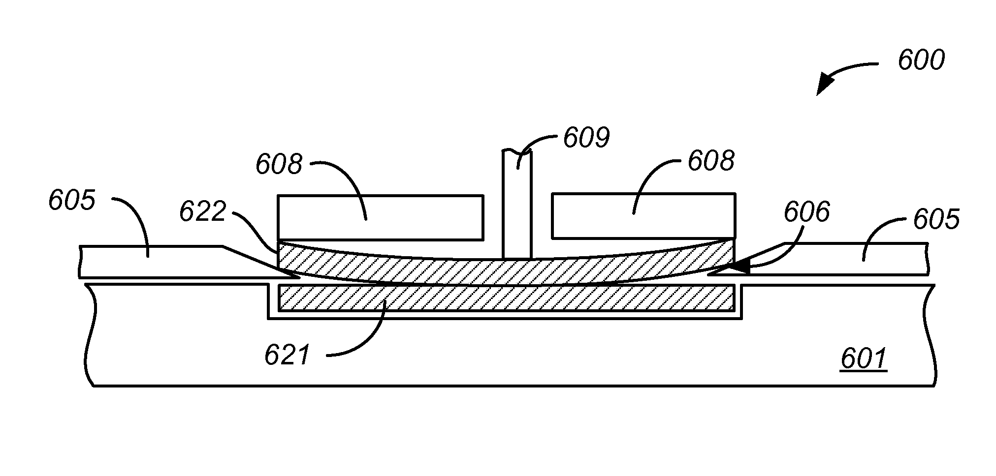
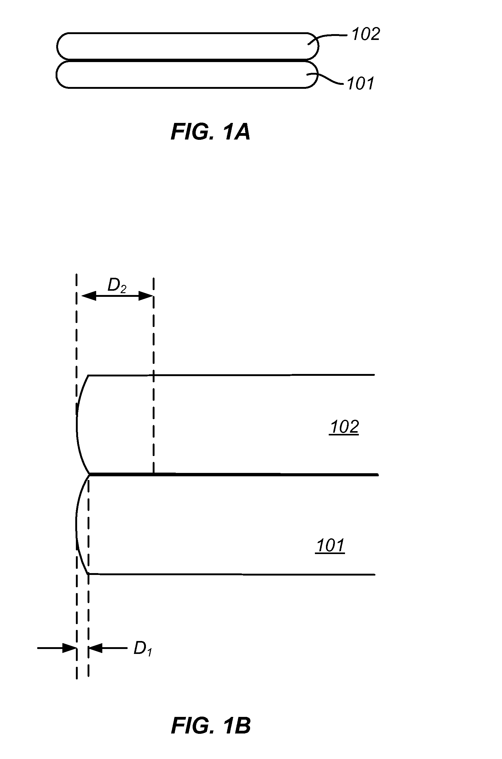
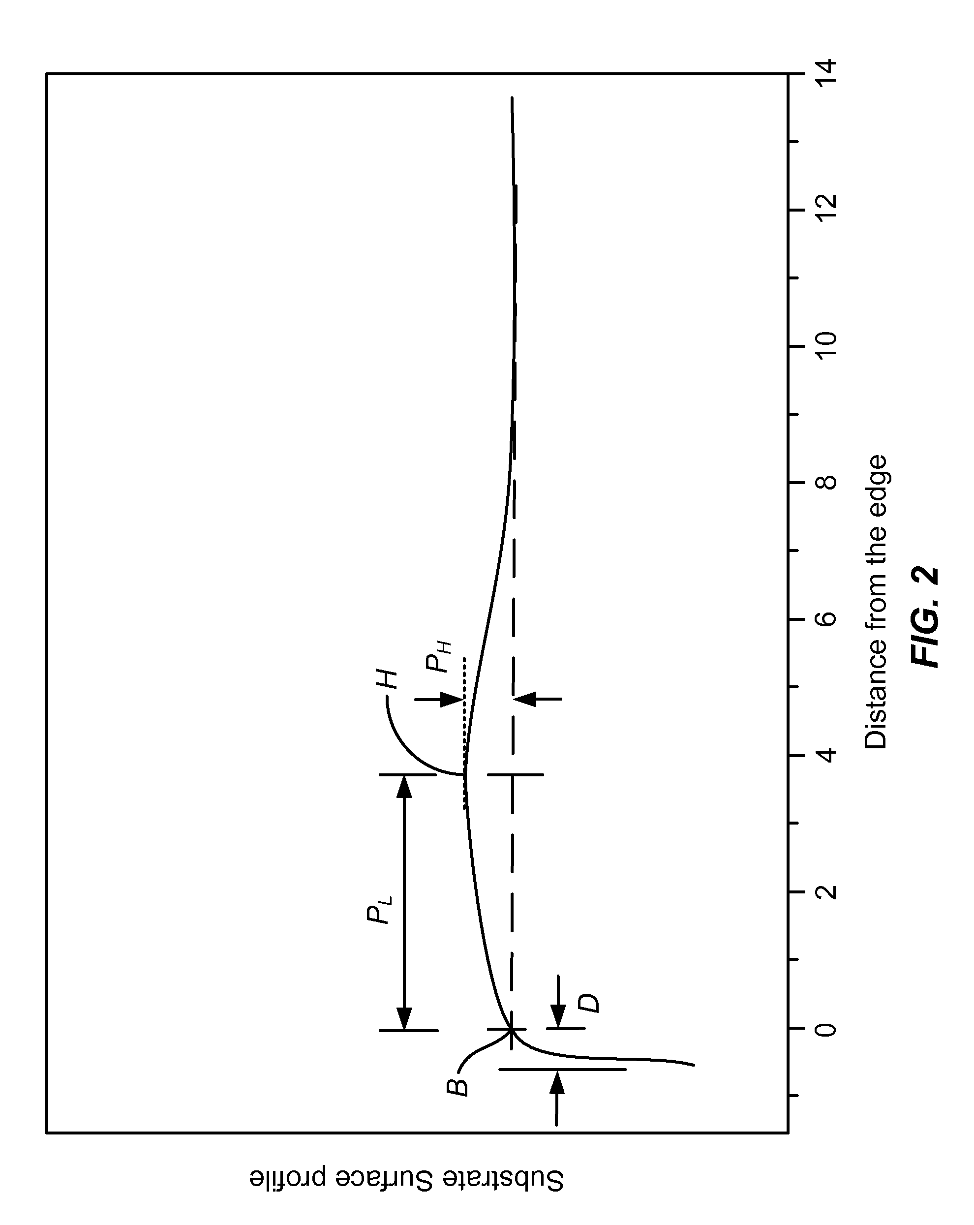
[0036]In accordance with embodiments of the present invention, a method for forming bonded substrates is provided. In one embodiment, the method includes determining a surface topographical characteristic that is related to the length of the non-bonded edge region, also known as the edge exclusion region, of bonded substrates. The method includes selecting suitable substrates according to the surface topographical characteristic. In another embodiment, the invention provides a method for forming bonded substrates by first forming a central contact between the substrates and then allowing the contact region to expand outward radially to the edge regions. Depending on the embodiments, edge exclusion regions in bonded substrates can be reduced using the methods provided in the present invention. In a specific embodiment, edge exclusion region as small as 1 mm in width has been obtained. Additionally, the invention also provides a simple and cost-effective apparatus for forming bonded s...


PUM

PropertyMeasurementUnit
lengthaaaaaaaaaa
characteristic lengthaaaaaaaaaa
lengthaaaaaaaaaa

Abstract

A method for forming bonded substrates includes providing a plurality of substrates, each of which having a top surface. A characteristic length for each of the plurality of substrates is determined by: determining a topographical profile of the top surface of the substrate from an interior portion to an edge portion along a radial direction, determining a highest point of the profile, and defining the characteristic length as a distance from the highest point to the edge portion. A first substrate and a second substrate are selected where at least one of the first or the second substrates has a characteristic length shorter than a predetermined length. The first substrate and the second substrate are brought into contact and form bonded substrates, with the top surface of the first substrate facing the top surface of the second substrate.

Description

BACKGROUND OF THE INVENTION[0001]The present invention is directed to method and apparatus for forming bonded substrates. More particularly, the invention provides a method and device for forming bonded substrates having small unbounded edge regions. Merely by way of example, techniques in accordance with the invention may be applied to forming bonded silicon wafers, e.g., for SOI (silicon on insulator) device applications. But it would be recognized that the invention has a much broader range of applicability. For example, the invention can be applied to forming bonded substrates for applications in power devices, thin film devices, as well as compound semiconductor devices.[0002]Bonded substrates are widely used in microelectronics fabrication. FIG. 1A is a cross-sectional view diagram illustrating bonded wafers. As shown, wafers 101 and 102 are bonded together by physical or chemical bonding forces. For example, an SOI wafer can be produced by bonding two silicon wafers together....

Claims


Application Information

Patent Timeline
Patent Type & Authority Applications(United States)
IPC IPC(8): B32B37/10B32B5/00
CPCB32B3/02B32B37/003B32B38/1866Y10T428/24802H01L21/67092Y10T156/17B32B2457/14B32B9/04
Inventor SOKOLOV, YURI V.ROY, DONALDHOOK, TYLER
Owner SEMICON COMPONENTS IND LLC
Why Eureka
Try Eureka