Touch screen sensor with low visibility conductors

a technology of conductors and touch screens, applied in the field of low visibility conductors, can solve the problems of sensor performance constraints, possible touch sensor designs, etc., and achieve the effects of reducing the visibility of micropattern elements, obscuring or reducing the visibility of conductive micropattern elements, and reducing the visibility of micropatterns

Active Publication Date: 2009-09-03
3M INNOVATIVE PROPERTIES CO
View PDF56 Cites 242 Cited by
  • Summary
  • Abstract
  • Description
  • Claims
  • Application Information

AI Technical Summary

Benefits of technology

[0004]A touch sensor or touch sensitive device having features to obscure or reduce the visibility of conductive micropattern elements.
[0005]In one embodiment, a touch-sensitive device is described, the touch sensitive device comprising a first visible light transparent substrate having a touch-interface surface and a display-interface surface, the touch-interface surface disposed toward touch input, and the display interface disposed toward the output of a display; a second visible light transparent substrate having a first surface and a second surface and also having a touch sensing area comprised of an electrically conductive micropattern disposed on or in the second visible light transparent substrate, wherein the micropattern includes conductors with width between about 1 and 10 micrometers; wherein the first surface of the second visible light transparent substrate is disposed toward the display-interface surface of the first visible light transparent substrate; and wherein the first visible light transparent substrate includes a feature that reduces the visibility of the micropattern.
[0006]In another embodiment, a touch screen sensor is described, the touch screen sensor comprising, within a touch sensing area, a electrically conductive micropattern disposed on or in a visible light transparent substrate, wherein the micropattern includes conductive traces with width between about 1 and 10 micrometers; one or more micropattern-obscuring features to reduce the visibility of the micropattern.

Problems solved by technology

This fact leads to a constraint on possible touch sensor designs and sensor performance, and necessitates such measures as expensive signal processing electronics or placement of additional electrodes to modify the electrical potential gradients.

Method used


Image

  • Touch screen sensor with low visibility conductors
  • Touch screen sensor with low visibility conductors
  • Touch screen sensor with low visibility conductors

Examples


example 1

[0146]A micropattern of thin film gold according to the following description is deposited onto a thin sheet of colorless glass (approximately 1 millimeter in thickness). The micropattern 240 is depicted in FIG. 11 and FIG. 12. The thickness or height of the gold layer is about 100 nanometers. The micropattern 240 involves a series of horizontal (x-axis) mesh bars 241 comprising horizontal narrow traces 242, the traces 242 measuring approximately 2 micrometers in width. Four of these horizontal mesh traces 242 are in electrical communication with a larger feature contact pad 260. The mesh bars measure approximately 6 millimeters in width. Accordingly, with thirteen evenly spaced traces 244 traversing a width (y-axis) of 6 millimeters and thirteen evenly spaced traces 242 traversing a length (x-axis) of 6 millimeters, the pitch of the square grid of traces is 500 micrometers. As depicted in FIG. 12, certain traces have breaks 250, measuring approximately 25 micrometers (exaggerated i...

example 2

[0147]A micropattern of thin film gold according to the following description is deposited onto a thin sheet of colorless glass (approximately 1 millimeter in thickness). The micropattern 340 is depicted in FIG. 15. The thickness of the gold is about 100 nanometers. The micropattern 340 has transparent conductive regions in the form of a series of interdigitated wedges or triangles. Each wedge is comprised of a mesh made up of narrow metallic traces 342, 344, the traces 342, 344 (see FIG. 15a-FIG. 15c) measuring approximately 2 micrometers in width. The mesh wedges measure approximately 1 centimeter in width at their base and approximately six centimeters in length. The pitch of the square grid of traces 342, 344 is 500 micrometers. Within selected regions of the mesh (see FIG. 15a-FIG. 15b), within a wedge, breaks 350 measuring approximately 25 micrometers in length are placed intentionally to affect the local sheet resistance within the wedge, for current passing along its long ax...

example 3

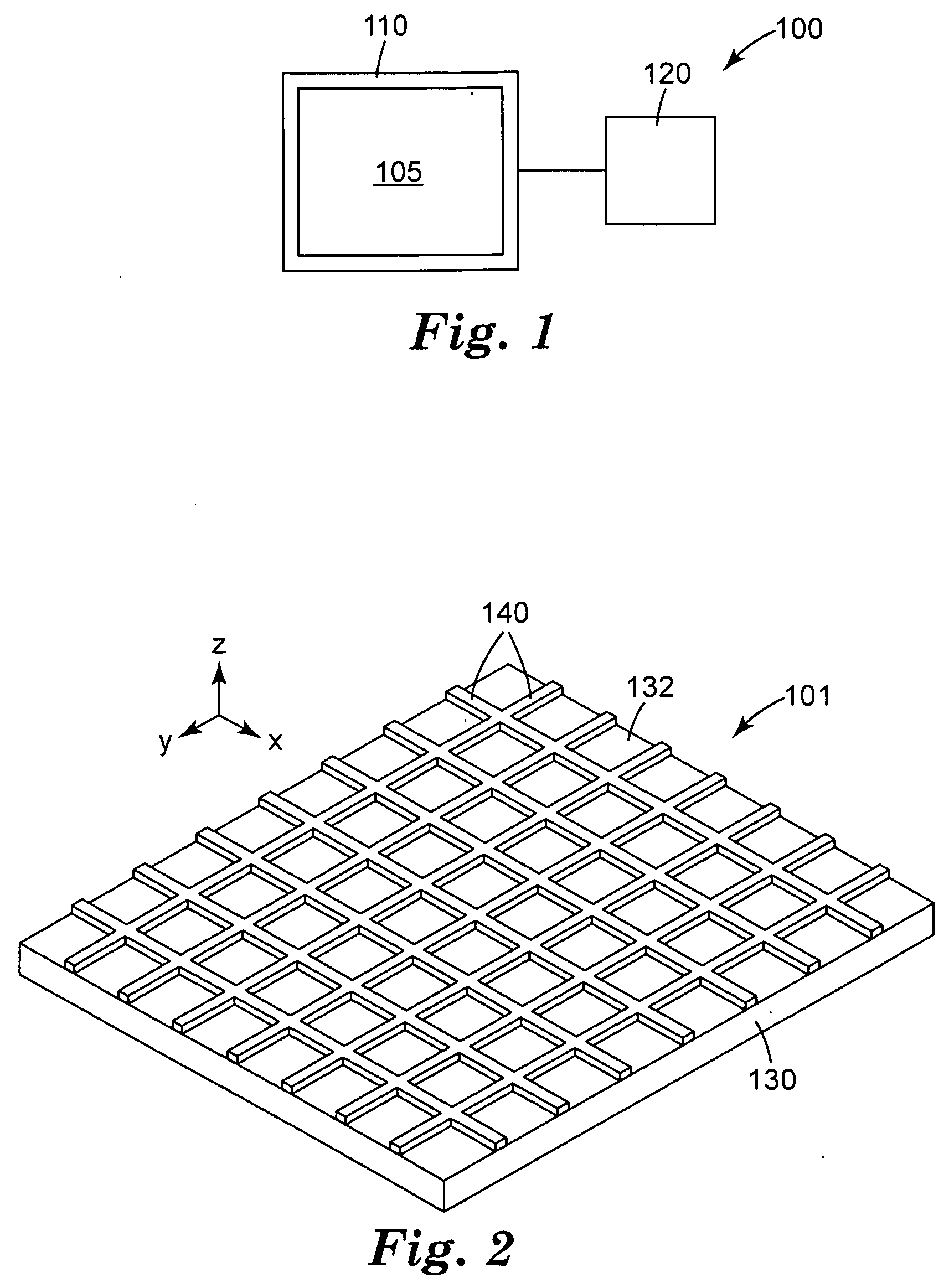
[0149]A transparent sensor element 400 for a touch screen sensor is illustrated in FIG. 17. The sensor element 400 includes two patterned conductor layers 410, 414, (e.g., an X axis layer and a Y axis layer) two optically clear adhesive layers 412, 416, and a base plate 418, laminated together and depicted as separated in FIG. 17 for clarity. Layers 410 and 414 include transparent conductive mesh bars where one layer is oriented in the x axis direction and the other layer is orientated in the y axis direction, with reference to FIG. 2. The base plate 418 is a sheet of glass measuring 6 centimeter by 6 centimeters in area and 1 millimeter in thickness. A suitable optically clear adhesive is Optically Clear Laminating Adhesive 8141 from 3M Company, St. Paul, Minn. For each of the X-layer and the Y-layer, a clear polymer film with a micropattern of metal is used. A micropattern of thin film gold according to the following description is deposited onto a thin sheet of PET. Suitable PET ...


PUM

PropertyMeasurementUnit
widthaaaaaaaaaa
widthaaaaaaaaaa
transparentaaaaaaaaaa

Abstract

A touch screen sensor with a conductive micropattern includes one or more features to obscure or reduce the visibility of the conductive micropattern.

Description

CROSS-REFERENCE TO RELATED APPLICATIONS[0001]This application claims the benefit of U.S. Provisional Application Nos. 61 / 032,269, filed Feb. 28, 2008, the disclosure of which is incorporated by reference herein in its entirety; 61 / 032,273, filed Feb. 28, 2008, the disclosure of which is incorporated by reference herein in its entirety; 61 / 085,496, filed Aug. 1, 2008, the disclosure of which is incorporated by reference herein in its entirety; 61 / 085,799, filed Aug. 1, 2008, the disclosure of which is incorporated by reference herein in its entirety; and 61 / 085,764, filed Aug. 1, 2008, the disclosure of which is incorporated by reference herein in its entirety.BACKGROUND[0002]Touch screen sensors detect the location of an object (e.g. a finger or a stylus) applied to the surface of a touch screen display or the location of an object positioned near the surface of a touch screen display. These sensors detect the location of the object along the surface of the display, e.g. in the plan...

Claims


Application Information

Patent Timeline
Patent Type & Authority Applications(United States)
IPC IPC(8): G06F3/041
CPCG06F3/044G06F2203/04112G06F3/045C23F1/14G06F3/0412G06F3/0445G06F3/0446
Inventor GEAGHAN, BERNARD O.HAGERMOSER, EDWARD S.
Owner 3M INNOVATIVE PROPERTIES CO
Why Eureka
Try Eureka