Imaging Device, Driving Method of the Same, Display Device and Electronic Apparatus

a display device and driving method technology, applied in the direction of instruments, television systems, television system scanning details, etc., can solve the problems of low layout efficiency and difficulty in ensuring an opening area in each pixel, and achieve the effect of reducing layout space, reducing frame region, and fewer control signals

Inactive Publication Date: 2009-09-03
JAPAN DISPLAY INC
View PDF5 Cites 6 Cited by
  • Summary
  • Abstract
  • Description
  • Claims
  • Application Information

AI Technical Summary

Benefits of technology

[0008]As described above, the present invention combines the driver circuits into a single circuit, thus ensuring reduced layout space over the conventional imaging devices. This contributes to reduced frame region. Further, the present invention uses fewer control signals and thus has fewer wirings. Still further, the driver circuits in the frame region on one side can be combined into a single circuit. This eliminates the need to provide wirings which straddle the driver circuits, thus ensuring high layout efficiency.

Problems solved by technology

This may make it difficult to secure an opening area in each pixel.
This may result in extremely low layout efficiency.

Method used


Image

  • Imaging Device, Driving Method of the Same, Display Device and Electronic Apparatus
  • Imaging Device, Driving Method of the Same, Display Device and Electronic Apparatus
  • Imaging Device, Driving Method of the Same, Display Device and Electronic Apparatus

Examples


Embodiment Construction

[0027]A description will be given below of an imaging device, a driving method of the same, a display device and an electronic apparatus according to the present invention with reference to the drawings.

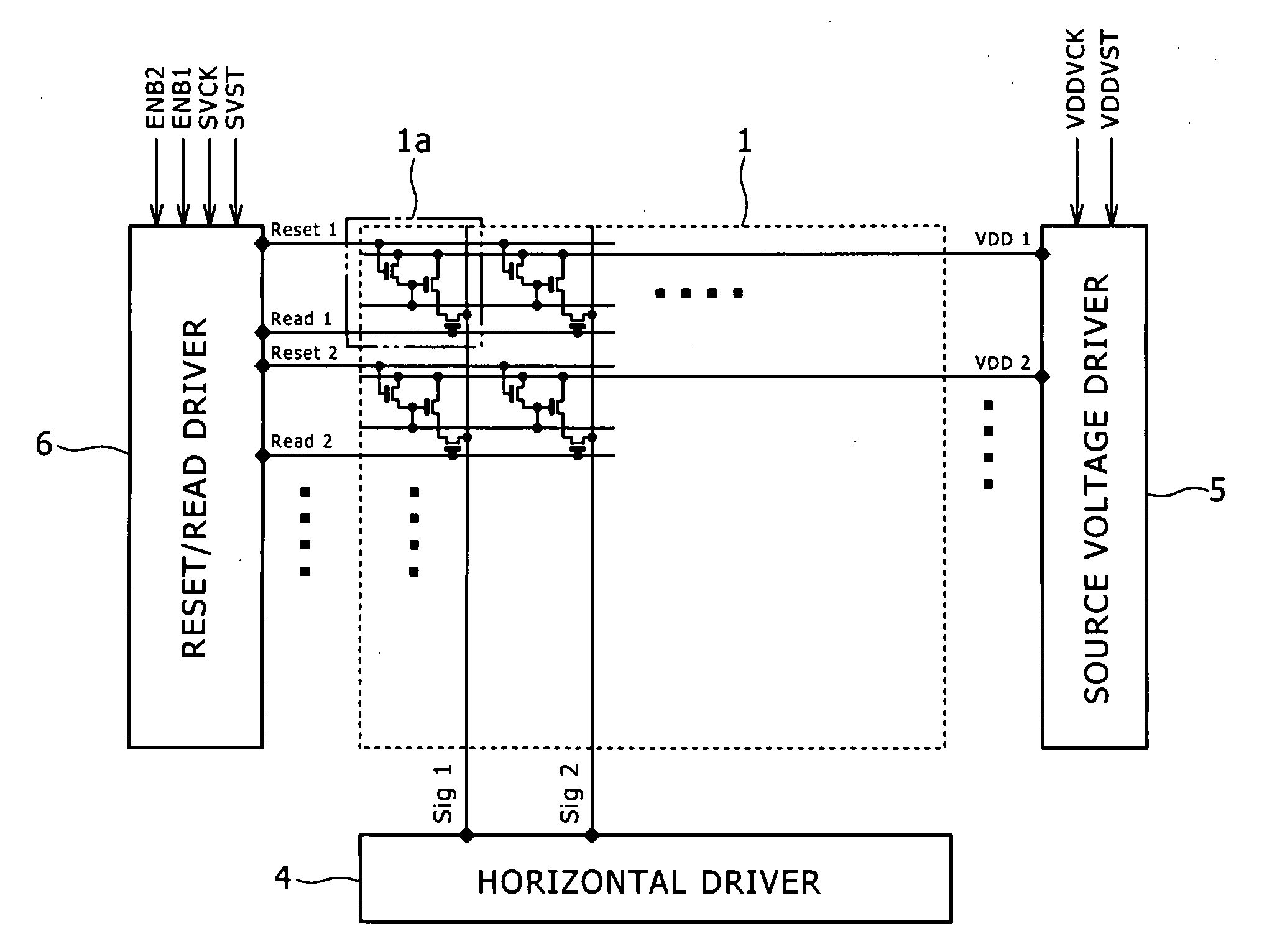
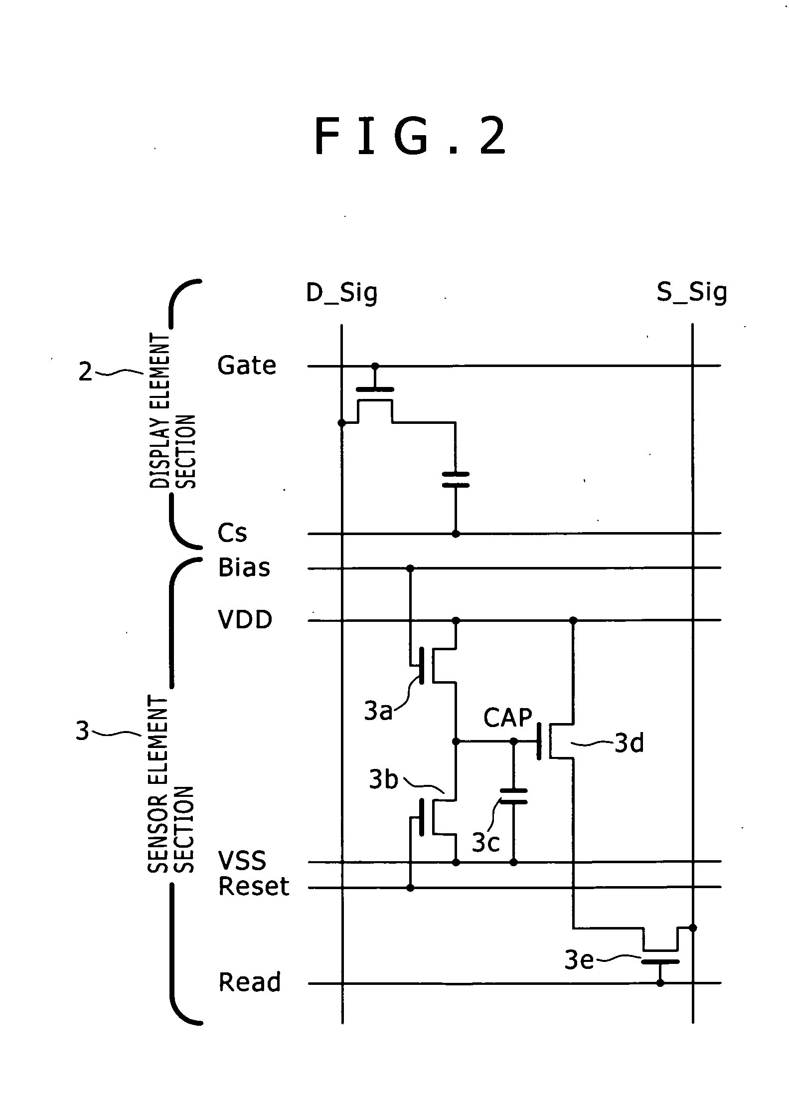
[0028]The schematic configuration of the imaging device according to the present invention will be described first. FIG. 1 is a circuit diagram illustrating an example of the schematic configuration of the imaging device according to the present invention. FIG. 2 is a circuit diagram illustrating an example of the major components included in the imaging device. FIG. 3 is a timing chart illustrating an example of the operation of the major components.

[0029]The imaging device described in the present embodiment includes a sensor group 1 as illustrated in FIG. 1. The sensor group 1 includes a plurality of pixel sections 1a arranged in a matrix. The sensor group 1 is configured to permit information entry using incident light on one hand and image display on the other hand. That is, the...


PUM


Abstract

In an imaging device including imaging elements, a driver configuration which does not require much layout space and ensures a reduced number of wirings is provided. The imaging device includes imaging elements 1 arranged in a matrix or in lines and a single driver circuit 6 disposed along the vertical direction of the matrix or along the direction in which the lines extend to control the driving of the imaging elements 1. Then, the driver circuit 6 serves the double function of a reset driver adapted to reset the imaging elements and a read driver adapted to read out the signals from the imaging elements.

Description

TECHNICAL FIELD[0001]The present invention relates to an imaging device having imaging elements, a driving method of the same, a display device and an electronic apparatus.BACKGROUND ART[0002]Typically, optoelectric conversion elements such as a CCD (Charge Coupled Devices) sensor, a CMOS (Complementary Metal Oxide Semiconductor) sensor and the like are widely known as imaging elements adapted to capture an image. In recent years, a combination of a thin film transistor (hereinafter abbreviated as “TFT”), capacitor and other components has been proposed to function as an optoelectric conversion element. An example thereof is, for example, a display device which includes liquid crystal display elements, the TFT adapted to function as an optoelectric conversion element and other components in each of pixels arranged in a matrix. The display device further includes a backlight or frontlight as a light source and displays an image by transmitting light from the light source through the ...

Claims


Application Information

Patent Timeline
Patent Type & Authority Applications(United States)
IPC IPC(8): G09G5/00G09G3/20H04N5/335H04N5/372H04N5/374H04N5/376
CPCH01L27/14609H04N5/376H04N3/1512H04N25/74
Inventor TERANISHI, YASUYUKINAKAJIMA, YOSHIHARUMATSUI, MASAFUMI
Owner JAPAN DISPLAY INC
Why Eureka
Try Eureka