
Method of forming crystalline layer, and thin film solar cell and method of fabricating the solar cell adopting the method of forming crystalline layer

Inactive Publication Date: 2009-09-10
SAMSUNG ELECTRONICS CO LTD +1
View PDF18 Cites 26 Cited by
  • Summary
  • Abstract
  • Description
  • Claims
  • Application Information

AI Technical Summary

Benefits of technology

[0008]Exemplary embodiments also relate to a high efficiency thin film solar cell, which is easily fabricated with low fabrication costs using an efficient crystallization of an amorphous layer, and a method of fabricating the thin film solar cell.

Problems solved by technology

The temperature of a thermal process is restricted by the thermal stability of any substrate materials.
If the substrate comprises a material that has low thermal stability, for example, glass or plastic, the substrate cannot be thermally processed at an ultra-high temperature.
Consequently, when a substrate of low thermal stability is used, crystallization of silicon is performed at a temperature that the substrate can sustain without substantial degradation, and as a result polycrystalline silicon of satisfactory quality cannot be obtained.
In addition, even when a thermal process is performed at a temperature that the substrate can sustain without degradation, the substrate still can be exposed to a locally high temperature, and thus the substrate may be damaged or may deform.
Accordingly, limits on process temperatures limit improvements in the quality of a crystalline thin film.

Method used


Image

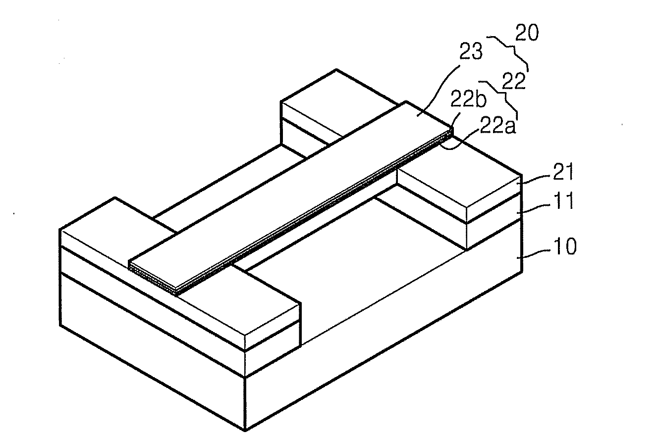
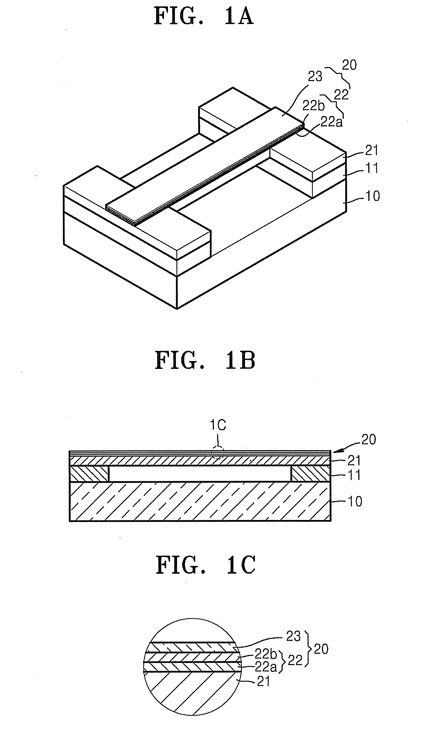
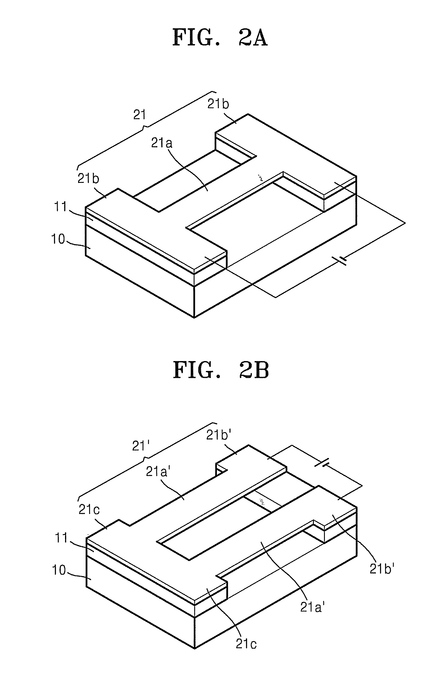
  • Method of forming crystalline layer, and thin film solar cell and method of fabricating the solar cell adopting the method of forming crystalline layer
  • Method of forming crystalline layer, and thin film solar cell and method of fabricating the solar cell adopting the method of forming crystalline layer
  • Method of forming crystalline layer, and thin film solar cell and method of fabricating the solar cell adopting the method of forming crystalline layer

Examples


Embodiment Construction

[0044]Described more fully hereinafter, with reference to the accompanying drawings, are embodiments of the disclosure. The disclosed embodiments should not be construed as limiting the claims to the exemplary embodiments shown. Rather, these embodiments are provided to convey the scope of the disclosure to one skilled in the art. In the drawings, the size and relative sizes of elements and regions may be exaggerated for clarity.

[0045]It will be understood that when an element or layer is referred to as being “on”, “disposed on”, “disposed”, or “between” another element or layer, it can be directly on, disposed on, disposed, or between the other element or layer, or intervening elements or layers can be present.

[0046]The terms “first,”“second,” and the like, “primary,”“secondary,” and the like, as used herein do not denote any order, quantity, or importance, but rather are used to distinguish one element, region, component, layer, or section from another. The terms “front”, “back”, ...


PUM


Abstract

A method of forming a crystalline layer includes: disposing a heating layer on a substrate, wherein the heating layer is separated from the substrate by a support structure; and forming a crystalline layer on the heating layer using heat generated from the heating layer.

Description

[0001]This application claims priority to Korean Patent Application No. 10-2008-0020584, filed on Mar. 5, 2008, and all the benefits accruing therefrom under 35 U.S.C. § 119, the contents of which in its entirety are incorporated herein by reference.BACKGROUND[0002]1. Field[0003]This disclosure relates to a thin film solar cell, and a method of fabricating the thin film solar cell.[0004]2. Description of the Related Art[0005]For commercialization of thin film solar cells, a method to improve fabrication efficiency of thin film solar cells, and reduce fabrication costs, is desirable. For commercial processes, polycrystalline silicon is preferred. The temperature of a thermal process is restricted by the thermal stability of any substrate materials. If the substrate comprises a material that has low thermal stability, for example, glass or plastic, the substrate cannot be thermally processed at an ultra-high temperature. Consequently, when a substrate of low thermal stability is used,...

Claims


Application Information

Patent Timeline
IPC IPC(8): H01L31/0248H01L31/024H01L31/0296H01L31/0304H01L31/0272H01L31/0352H01L31/0368
CPCH01L31/022425H01L31/035281H01L31/0368H01L31/0392H01L31/068H01L31/072Y02E10/547H01L31/1804H01L31/1836H01L31/1852H01L31/1872Y02E10/544Y02E10/548H01L31/075Y02P70/50H01L31/18H01L31/0445
Inventor PARK, YOUNGJUNCHOI, JUNHEENAM, JUNGGYU
Owner SAMSUNG ELECTRONICS CO LTD
Learn More