

LED chip package structure with a high-efficiency heat-dissipating substrate and method for making the same
- Summary
- Abstract
- Description
- Claims
- Application Information
AI Technical Summary
Benefits of technology
Problems solved by technology
Method used
Image

Examples
first embodiment
[0033]Referring to FIGS. 2, 2A to 2D, and 2E, the present invention provides a method of packaging LED chips package structure with a high-efficiency heat-dissipating substrate.
[0034]The method of the present invention includes: referring to FIGS. 2 and 2A, providing a substrate unit 1 that has a positive substrate 10, a negative substrate 11, and a plurality of bridge substrates 12 separated from each other and disposed between the positive substrate 10 and the negative substrate 11 (S200). The substrate unit 1 can be a PCB (Printed Circuit Board), a flexible substrate, an aluminum substrate, a ceramic substrate, or a copper substrate.
[0035]Referring to FIGS. 2 and 2B, the method of the first embodiment further includes: filling an adhesive body 2 between the positive substrate 10, the negative substrate 11 and the bridge substrates 12 in order to connect and fix the positive substrate 10, the negative substrate 11 and the bridge substrates 12 together (S202). The adhesive body 2 c...
second embodiment
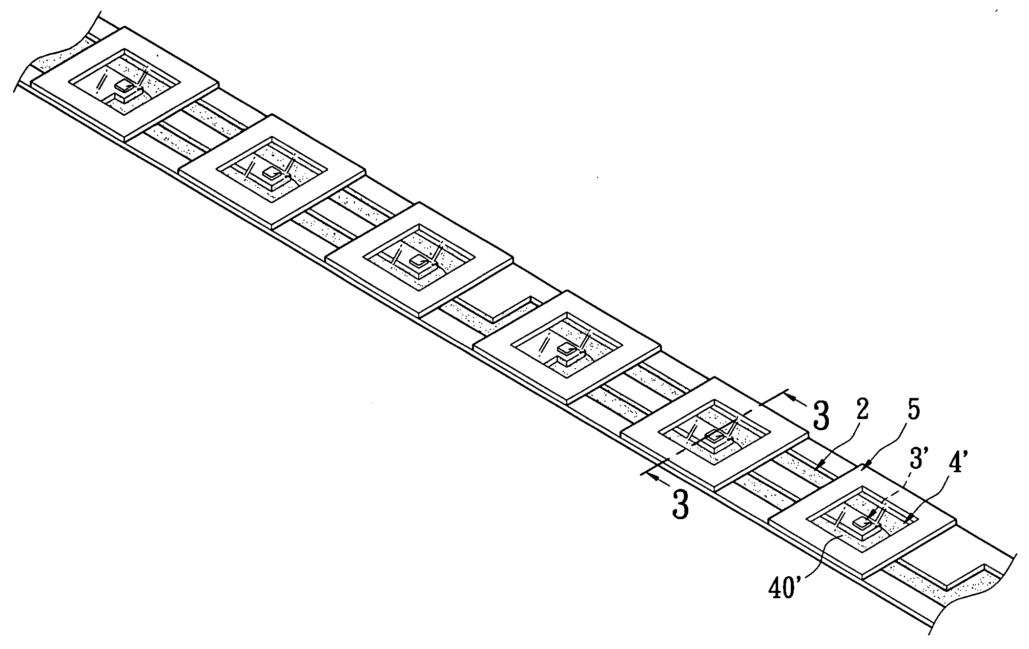
[0039]Referring to FIGS. 3, 3A and 3B, after the step S304, the method of the second embodiment further includes: respectively covering the LED chips 3′ with a plurality of transparent bodies 4′ (S306), and then respectively disposing a plurality of frame layers 5 around the packages bodies 4′ in order to form the light-projecting surfaces 40′ on the package bodies 4′ and the light-projecting surfaces 40′ corresponding to the LED chips 3′ (S308). Moreover, each LED chip 3′ is used for generating white light, for example a red LED, a green LED and a blue LED are mated to generate white light. Each transparent body 4′ can be made of transparent silicon or transparent epoxy.
[0040]Hence, the difference between the second embodiment and the first embodiment is that: in the second embodiment, each LED chip 3′ is used for generating white light (for example a red LED, a green LED and a blue LED are mated to generate white light), so the transparent body 4′ can be transparent.
[0041]Referrin...
PUM
 Abstract
Description
Claims
Application Information