Packaging method of image sensing device
- Summary
- Abstract
- Description
- Claims
- Application Information
AI Technical Summary
Benefits of technology
Problems solved by technology
Method used
Image
Examples
Embodiment Construction
[0020]The present invention will now be described more specifically with reference to the following embodiment. It is to be noted that the following descriptions of the preferred embodiment of this invention are presented herein for purpose of illustration and description only; it is not intended to be exhaustive or to be limited to the precise form disclosed.
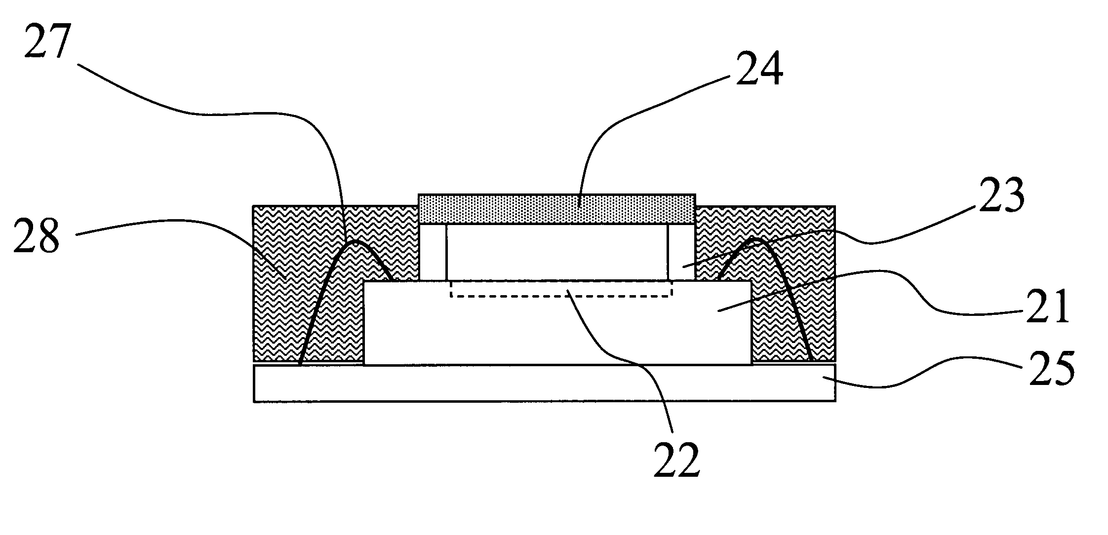
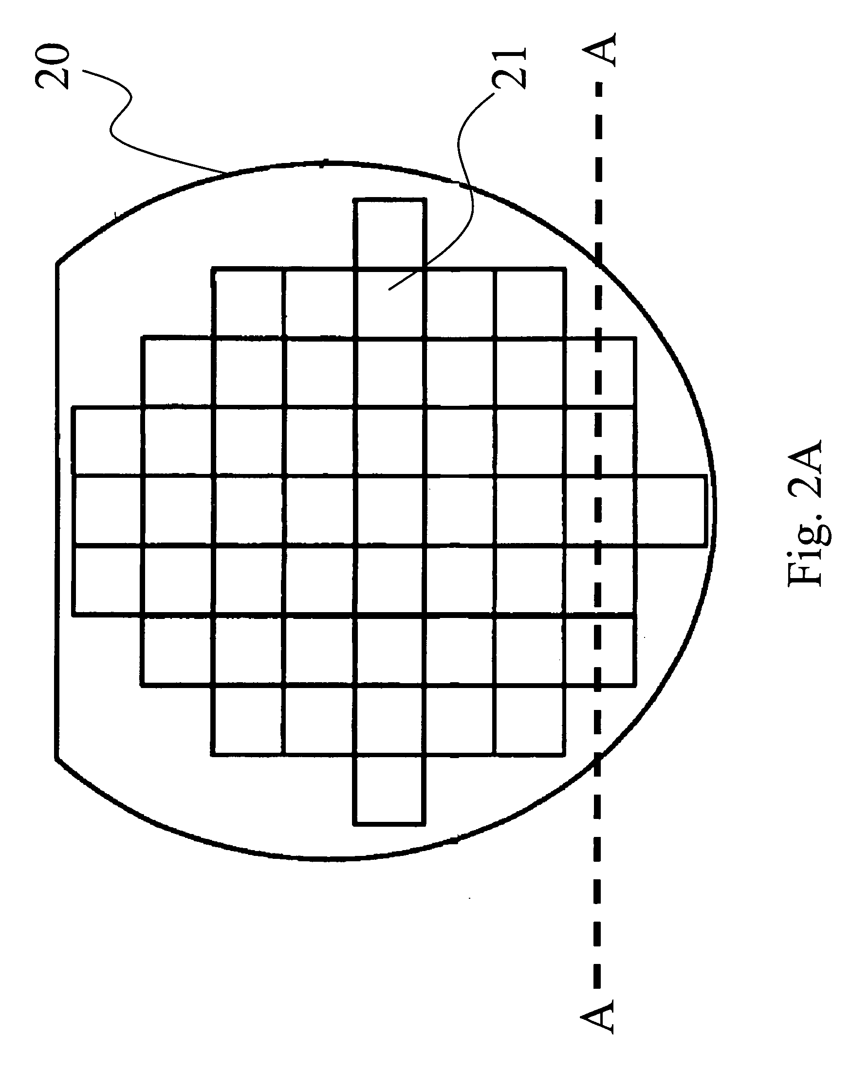
[0021]Please refer to FIGS. 2A-2I. They illustrate an embodiment of a packaging method for an image sensing device according to the present invention. FIG. 2A is a top view diagram of an integrated circuit (IC) wafer 20. The wafer 20 contains at least one image sensing module 21 which is also known as “die”. Usually, a wafer has hundreds or thousands of image sensing modules depending on the size of each image sensing module. The smaller size of each image sensing module is, the more modules the wafer can accommodate. FIG. 2B is a cross-sectional diagram cut along line A-A in FIG. 2A showing five image sensing modules 21.
[0022]...
PUM
 Abstract
Description
Claims
Application Information


