Image display unit

Inactive Publication Date: 2011-02-01
SONY CORP
View PDF47 Cites 167 Cited by
  • Summary
  • Abstract
  • Description
  • Claims
  • Application Information

AI Technical Summary

Benefits of technology

[0016]The present invention provides an improved image display unit including light emitting devices and methods of producing same. In this regard, the present invention provides improved image display units having enhanced characteristics such as resolution, image quality, and luminous efficiency, while facilitating formation of a large-s

Problems solved by technology

Each of the above-described image display units, however, has drawbacks in terms of characteristics such as resolution, luminance, light output/power efficiency, and image quality, and further, in terms of screen size and production costs.
Additionally, since the cost per each pixel is raised, the production costs become high, in particular, for an image display unit having a large screen.
Accordingly, to improve the production yield, the process control must be strictly performed, and therefore, the production costs are increased when producing a liquid crystal display unit having a large screen.
Further, liquid crystal display units have a viewing angle dependence in which the contrast or tint varies depending on a viewing angle, and also experience a response speed delay when one color is changed to another color.
Accordingly, plasma display units have low luminous efficiency and large power consumption.
Further, external light is reflected from phosphors, thereby degrading the contrast.
Accordingly, each of the above-described image display units make it difficult to form a large-sized screen, are high in production costs, and

Method used


Image

  • Image display unit
  • Image display unit
  • Image display unit

Examples


Embodiment Construction

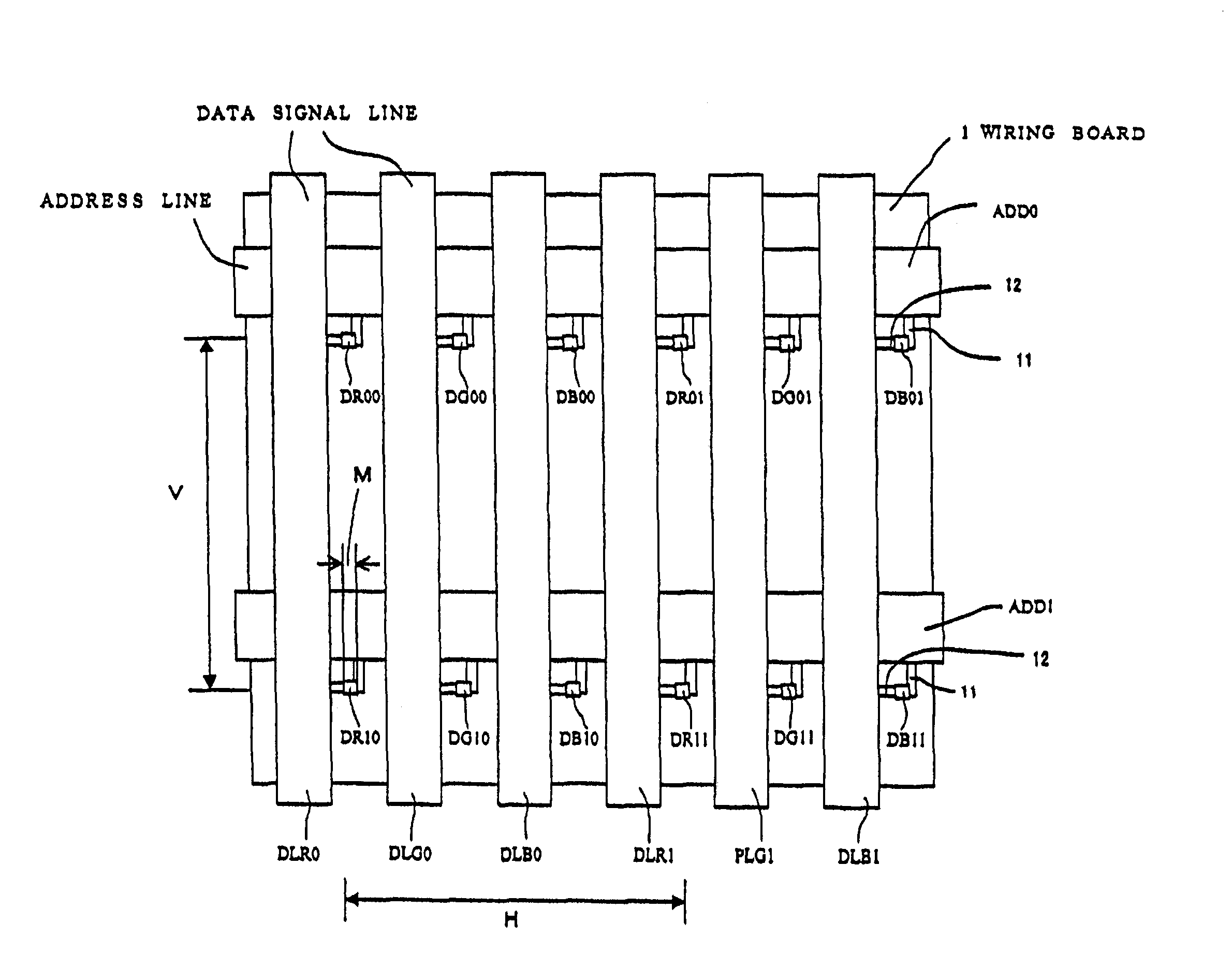
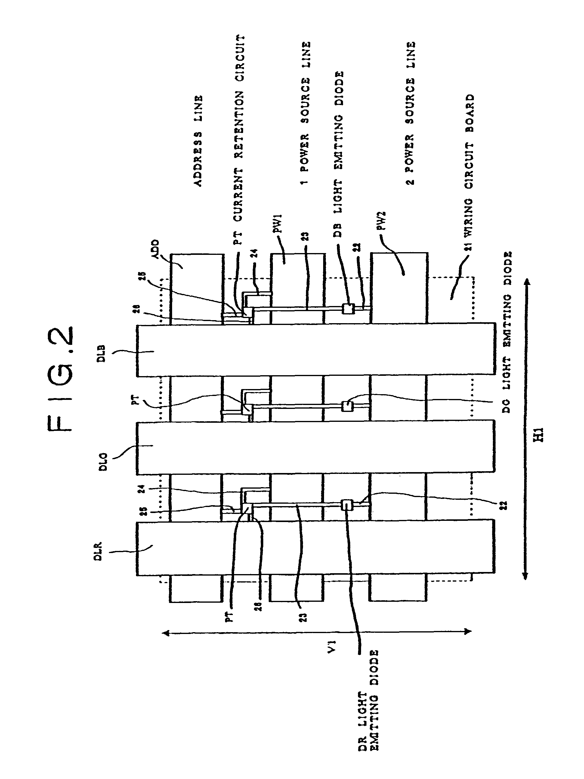
[0129]The present invention provides an image display unit including light emitting devices and methods of producing same. The present invention provides methods of arraying devices such that, for example, the image display unit of the present invention can be manufactured with reduced production time and costs while providing an image display unit with enhanced characteristics, such as resolution, image quality, and luminous efficiency.

[0130]In a method of arraying devices and a method of producing an image display unit according to an embodiment of the present invention, two-step transfer is performed by transferring devices formed on a first substrate at a high density onto a temporary or temporarily holding member such that the devices are spaced from each other with a pitch larger than a pitch of the devices arrayed on the first substrate, and further transferring the devices held on the temporarily holding member onto a second board such that the devices are spaced from each o...


PUM


Abstract

An image display unit and a method of producing the image display unit, wherein the image display unit includes an array of a plurality of light emitting devices for displaying an image, and wherein the method of producing the image display unit employs, for example, a space expanding transfer, whereby a first transfer step includes transferring the devices arrayed on a first substrate to a temporary holding member such that the devices are spaced from each other with a pitch larger than a pitch of the devices arrayed on the first substrate, a second holding step includes holding the devices on the temporary holding member, and a third transfer step includes transferring the devices held on the temporary holding member onto a second board such that the devices are spaced from each other with a pitch larger than the pitch of the devices held on the temporary holding member.

Description

CROSS REFERENCES TO RELATED APPLICATIONS[0001]This patent application is a divisional of U.S. application Ser. No. 10 / 066,423, filed on Jan. 30, 2002 now U.S. Pat. No. 6,613,610, which is a continuation of International Application No. PCT / JP01 / 06213 with an international filing date of Jul. 18, 2001. The present application claims priority to Japanese Patent Application No. P2000-217953 filed on Jul. 18, 2000; Japanese Patent Application P2000-217988 filed on Jul. 18, 2000; Japanese Patent Application No. P2000-396225 filed on Dec. 26, 2000; and Japanese Patent Application No. P2001-200113 filed on Jun. 29, 2001. The above-referenced patent applications are incorporated herein by reference to the extent permitted in law.BACKGROUND OF THE INVENTION[0002]The present invention generally relates to image display units and methods of producing same. More specifically, the present invention relates to an image display unit including light emitting devices and methods of producing same.[0...

Claims


Application Information

Patent Timeline
IPC IPC(8): H01L33/00G09F9/33G09F9/30G09F9/35H01L21/20H01L21/60H01L21/68H01L21/77H01L25/075H01L27/12H01L27/15H01L33/06H01L33/24H01L33/32H01L33/40H01L33/48
CPCH01L21/6835H01L24/18H01L24/82H01L25/0753H01L27/156H01L33/0079H01L33/24H01L21/2007G02F2001/13613H01L2224/81136H01L24/16H01L24/81H01L27/12H01L27/1214H01L27/1266H01L2221/6835H01L2221/68354H01L2221/68359H01L2221/68368H01L2224/16H01L2224/18H01L2224/48091H01L2224/48227H01L2224/81001H01L2924/01002H01L2924/01004H01L2924/01012H01L2924/01013H01L2924/01015H01L2924/01025H01L2924/01029H01L2924/0103H01L2924/01032H01L2924/01033H01L2924/01039H01L2924/01046H01L2924/01049H01L2924/01074H01L2924/01075H01L2924/01078H01L2924/01079H01L2924/01082H01L2924/10329H01L2924/19041H01L2924/19043H01L2924/30105H01L2924/3025H01L33/0095H01L2924/01005H01L2924/01006H01L2924/01023H01L2924/01024H01L2924/01047H01L2924/01087H01L2924/014H01L2924/12041Y10S438/982H01L2924/00014H01L2924/15788H01L2924/181H01L2924/12042H01L2924/12036H01L2224/05573H01L2224/05568H01L2224/16245H01L2924/3512H01L2224/04105H01L2224/32225H01L2224/73267H01L2224/92244H01L21/568H01L24/24H01L2224/06102H01L2224/1703H01L33/0093G02F1/13613H01L2924/00H01L2224/05599H01L21/20H01L27/15G09F9/33
Inventor IWAFUCHI, TOSHIAKIOOHATA, TOYOHARUDOI, MASATO
Owner SONY CORP
Why Eureka
Try Eureka