

Structure and method for coupling signals to and/or from stacked semiconductor dies
- Summary
- Abstract
- Description
- Claims
- Application Information
AI Technical Summary
Problems solved by technology
Method used
Image

Examples
Embodiment Construction
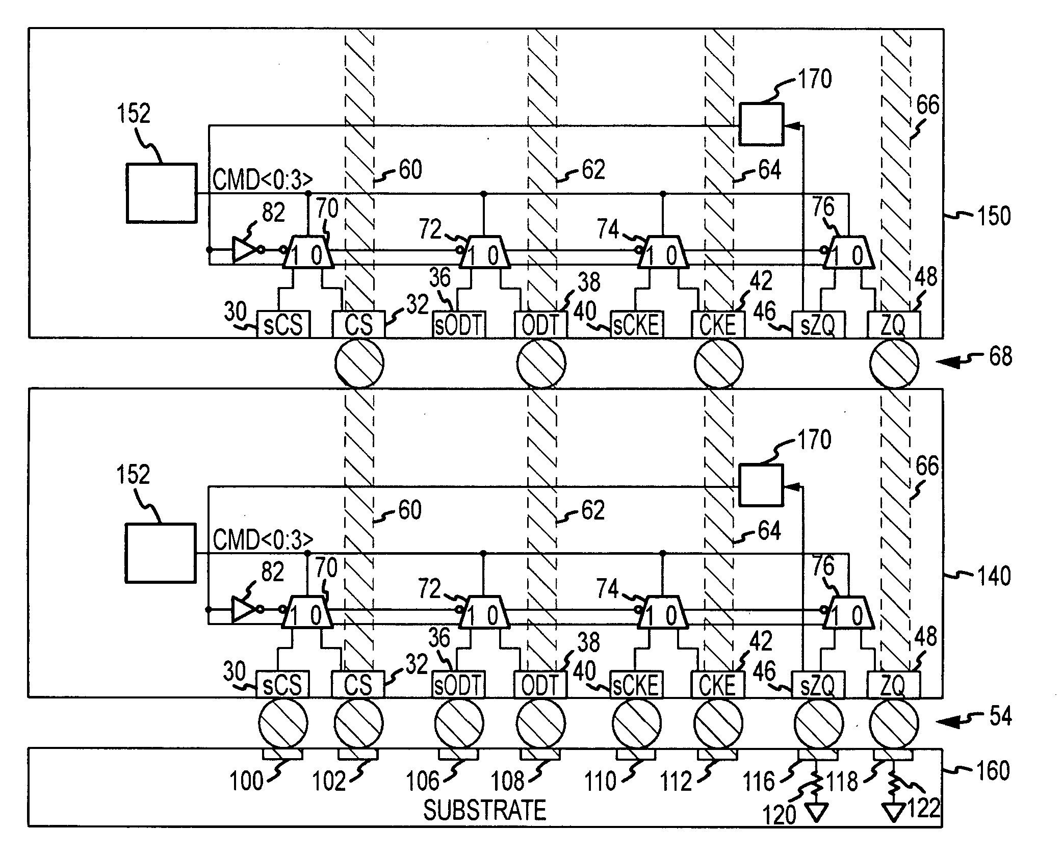
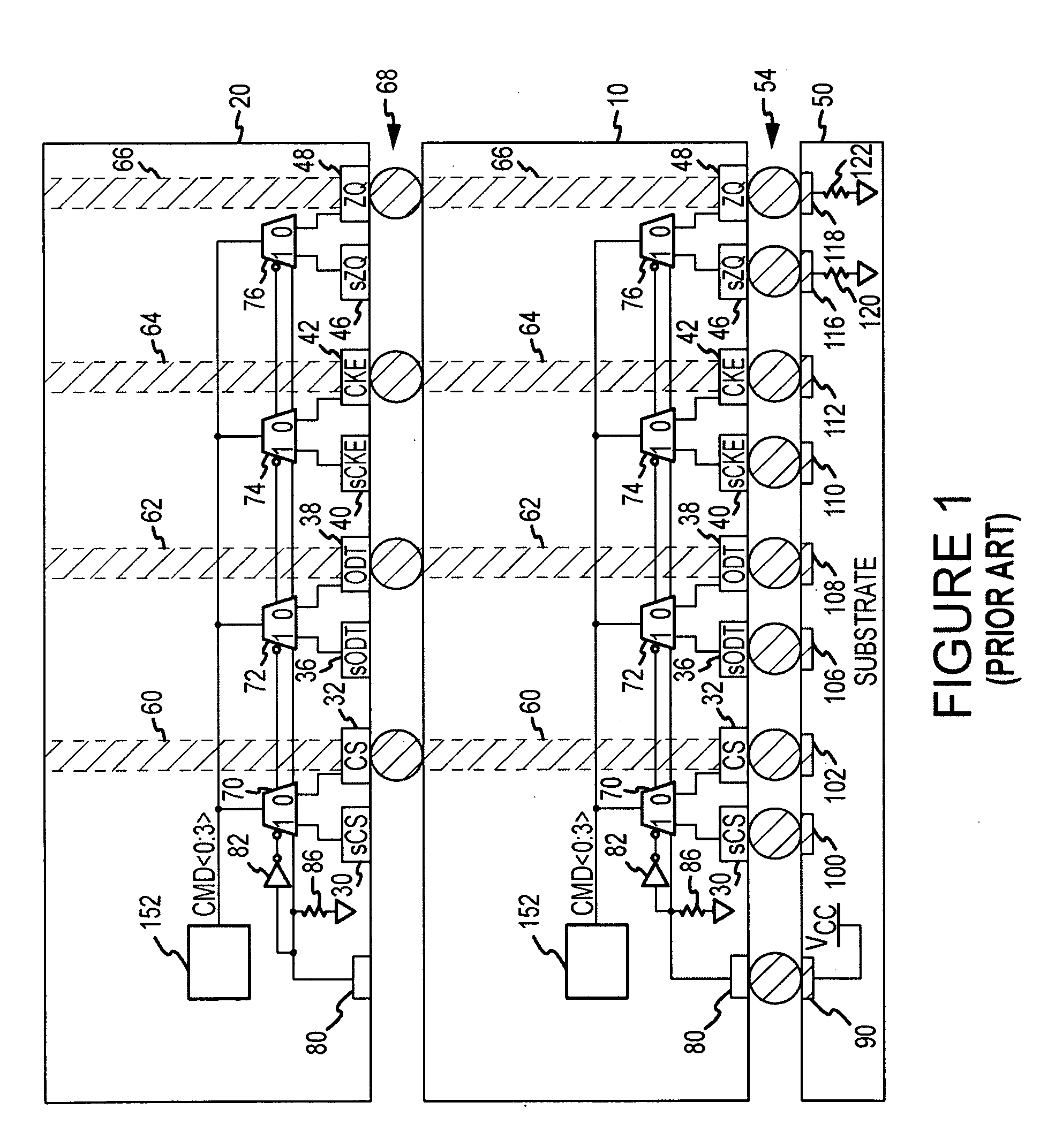
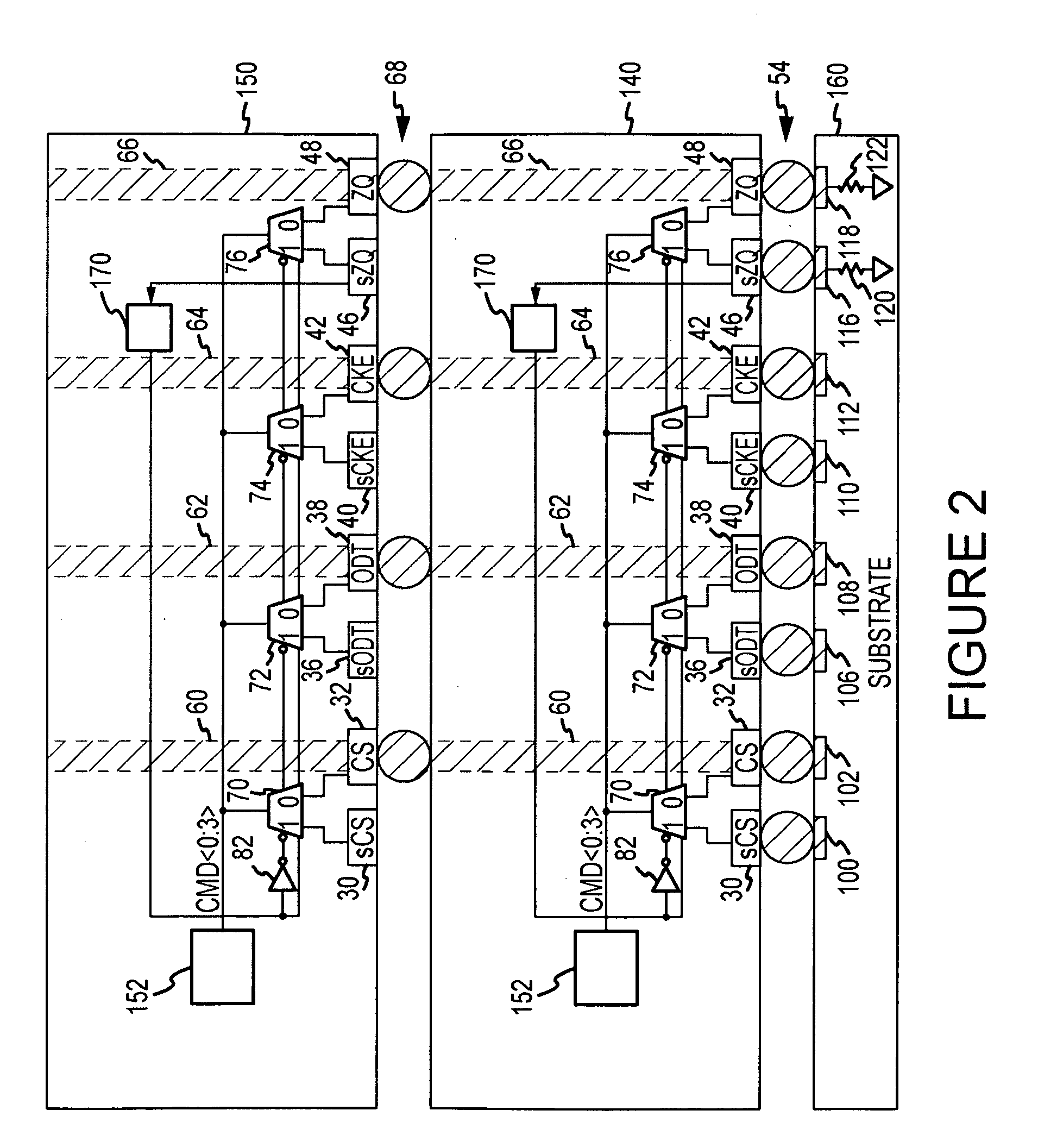
[0009]A cross-section of a pair of stacked dies 10, 20 using a conventional arrangement is shown in FIG. 1. The dies 10, 20 are identical to each other, and they have therefore been provided with the same reference numerals. Each of the dies 10, 20 include a plurality of bonding pads, although only the bonding pads for 4 signals are shown in FIG. 1. Specifically, the dies 10, 20 include a pair of pads 30, 32 for receiving respective chip select (sCS, CS) signals, a pair of pads 36, 38 for receiving respective on-die termination (sODT, ODT) signals, a pair of pads 40, 42 for receiving respective clock enable (sCKE, CKE) signals, and a pair of pads 46, 48 for coupling to respective known impedances (sZQ, ZQ) for use in calibrating the termination impedance of data output buffers (not shown) that output signals to data bus pads (not shown). The pads 30-48 are coupled to respective conductors on a substrate 50 through a grid of conductive balls, generally indicated at 54, which are know...
PUM
 Abstract
Description
Claims
Application Information