Reflective mask blank, reflective mask, method of inspecting reflective mask, and method for manufacturing the same

a reflective mask and blank technology, applied in the field of reflective masks, can solve the problems of difficult and necessary changes in the optical system of the inspection apparatus, and achieve the effects of high detection accuracy, high detection accuracy, and accurate and rapid operation

Active Publication Date: 2009-09-17
RENESAS ELECTRONICS CORP +1
View PDF5 Cites 28 Cited by
  • Summary
  • Abstract
  • Description
  • Claims
  • Application Information

AI Technical Summary

Benefits of technology

[0013]According to the present invention, since an absorptive layer is formed directly on a substrate and the other side of the substrate is exposed in an alignment region, a multilayer, an intermediate layer and a conductive layer are not formed in the alignment region. Hence, when a reflective mask is prepared from the reflective mask blank of the present invention, it is possible to obtain a reflective mask capable of detecting an alignment mark by transmission. In such a reflective mask, an alignment mark may be detected with good contrast, and highly accurate positional arrangement is feasible in inspecting a circuit pattern of the reflective mask or in correcting a circuit pattern of the reflective mask.
[0024]According to the present invention, there is brought about an effect by which an alignment mark may be detected with good contrast by transmission, and highly accurate positional arrangement is feasible in inspecting a circuit pattern of a reflective mask and in correcting a circuit pattern of a reflective mask.

Problems solved by technology

In this case, however, alteration in the optical system of an inspection apparatus is necessary and not easy.

Method used


Image

  • Reflective mask blank, reflective mask, method of inspecting reflective mask, and method for manufacturing the same
  • Reflective mask blank, reflective mask, method of inspecting reflective mask, and method for manufacturing the same
  • Reflective mask blank, reflective mask, method of inspecting reflective mask, and method for manufacturing the same

Examples


first embodiment

1. First Embodiment

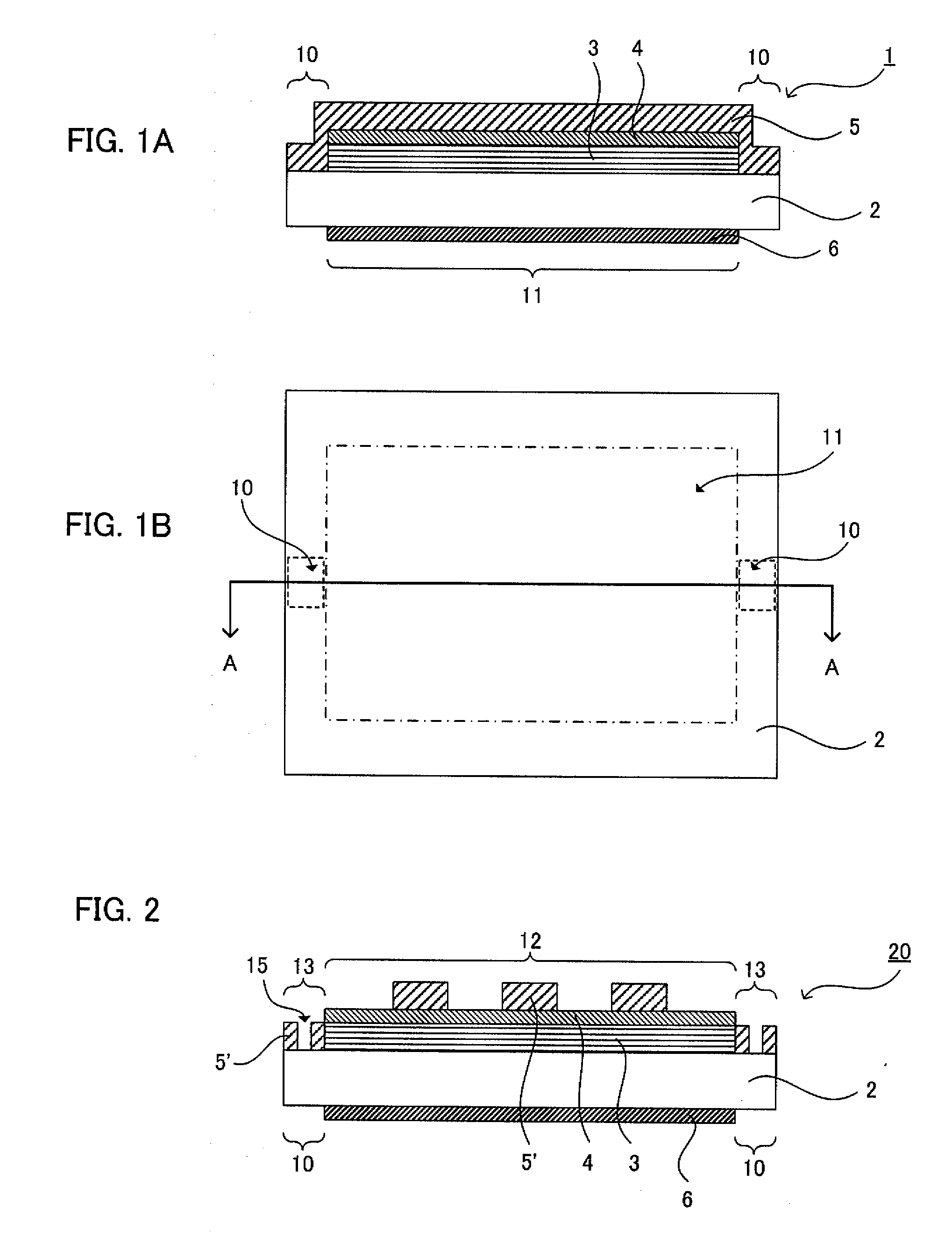
[0087]The reflective mask in the first embodiment of the invention is a reflective mask comprising a substrate, a multilayer formed on one side of the substrate, an intermediate layer formed on the multilayer, an absorber formed in pattern on the substrate on which the multilayer and the intermediate layer are formed, and a conductive layer formed on the other side of the substrate, wherein the pattern of the absorber constitutes a circuit pattern and an alignment mark, the other side of the substrate is exposed in an alignment region where the alignment mark is provided, the alignment mark is constituted of the absorber and an opening, and the opening of the alignment mark is formed directly on the substrate.

[0088]According to this embodiment, the side of the substrate on which the conductive layer is formed is exposed in the alignment region, the conductive layer is not formed in the alignment region, the opening of the alignment mark is formed directly on the s...

second embodiment

2. Second Embodiment

[0137]The reflective mask in the second embodiment of the invention is a reflective mask comprising a substrate, a multilayer formed on one side of the substrate, an intermediate layer formed on the multilayer, an absorber formed in pattern on the substrate on which the multilayer and the intermediate layer are formed, and a conductive layer formed on the other side of the substrate, wherein the pattern of the absorber constitutes a circuit pattern and an alignment mark, and in an alignment region where the alignment mark is provided, the other side of the substrate is exposed, and the alignment mark is formed on the intermediate layer.

[0138]The reflective mask in this aspect will be described by reference to the drawings.

[0139]FIG. 5 is a schematic cross-sectional view showing one example of the reflective mask in this aspect. In the reflective mask 20 illustrated in FIG. 5, a multilayer 3 and an intermediate layer 4 are laminated in this order on a substrate 2,...

example 1

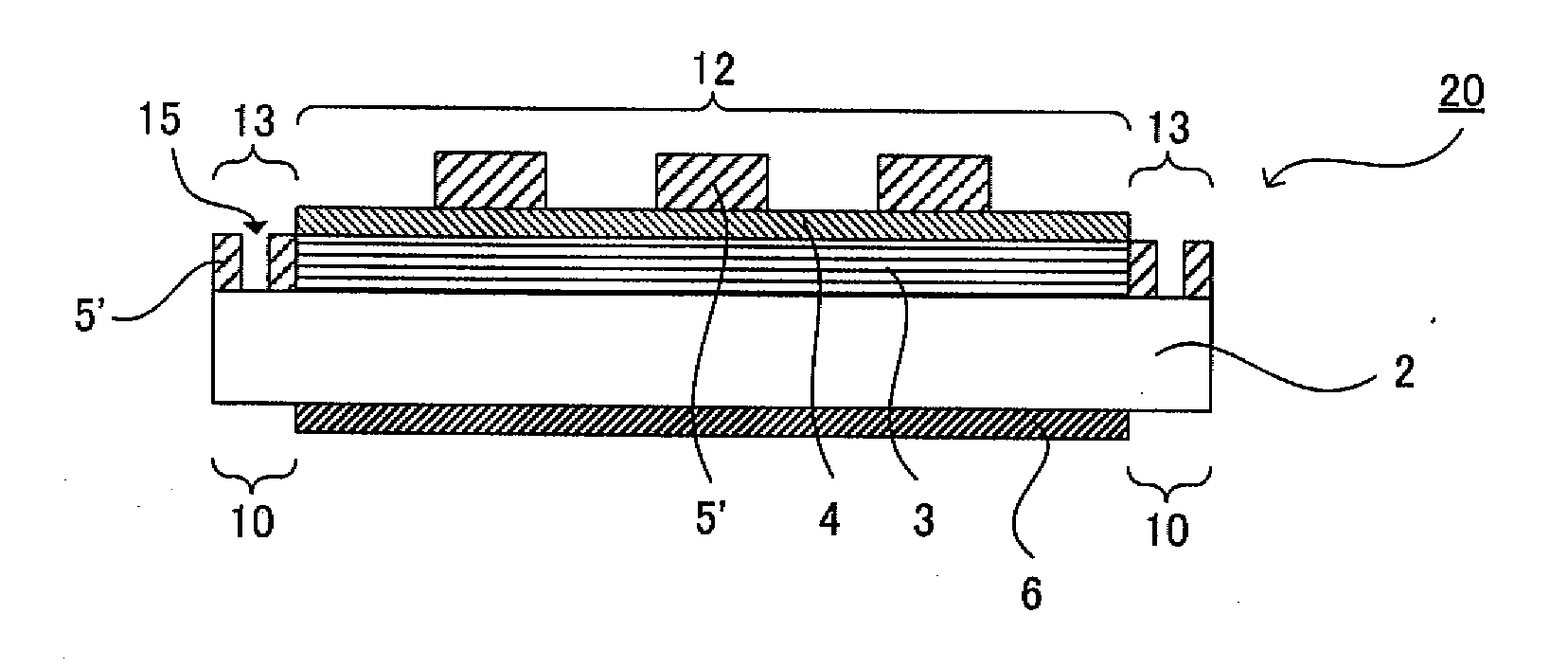
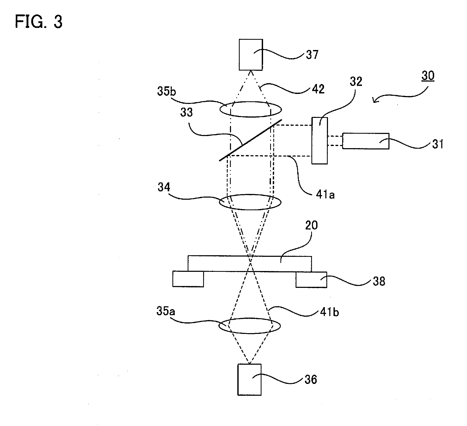
[0176]FIG. 4 is a cross-sectional view showing one aspect of the reflective mask according to the present invention. In this reflective mask, a multilayer 3 is formed as a reflective part on substrate 2, an intermediate layer 4 for the purpose of protecting the multilayer and of assisting pattern formation is formed on the multilayer 3, and a circuit pattern 12 as a non-reflective part, and an absorber 5′ constituting an alignment mark 13, are formed on the intermediate layer 4. On the other side of the substrate 2, a conductive layer 6 is formed in a region other than the alignment mark. In FIG. 4, the intermediate layer and the multilayer were removed from the portion of the opening 15 of the alignment mark by dry etching via FIB or EB system or via a resist process. The alignment mark was thereby composed of the absorber formed on the intermediate layer and the opening formed directly on the substrate. Hereinafter, an example of mask alignment using a transmission optical system ...


PUM

PropertyMeasurementUnit
thicknessaaaaaaaaaa
thicknessaaaaaaaaaa
thicknessaaaaaaaaaa

Abstract

A main object of the invention is to provide a reflective mask for EUV lithography, which may detect an alignment mark by transmission. The invention achieves the object by providing a reflective mask comprising a substrate, a multilayer formed on one side of the substrate, an intermediate layer formed on the multilayer, an absorber formed in pattern on the substrate on which the multilayer and the intermediate layer are formed, and a conductive layer formed on the other side of the substrate, wherein the pattern of the absorber constitutes a circuit pattern and an alignment mark, and in an alignment region where the alignment mark is provided, the other side of the substrate is exposed.

Description

BACKGROUND OF THE INVENTION[0001]1. Field of the Invention[0002]The present invention relates to a reflective mask used in extreme ultra violet (EUV) lithography.[0003]2. Description of the Related Art[0004]An inspection process wherein the accurate formation of a circuit pattern is inspected is usually conducted in a method for manufacturing a reflective mask for EUV lithography. In this inspection process, the accurate formation of a circuit pattern is inspected by irradiating a reflective mask with inspection light and detecting reflected light from the reflective mask. In the inspection process, defects may be easily detected when the ratio (contrast) of the reflectance of an absorber to the reflectance of a layer below the absorber (for example, a multilayer, a capping layer, or a buffer layer) is high.[0005]In the inspection process, positional alignment between a reflective mask and an inspection apparatus is usually conducted for inspecting a circuit pattern. In the reflecti...

Claims


Application Information

Patent Timeline
Patent Type & Authority Applications(United States)
IPC IPC(8): G03F1/00G03F1/22G03F1/24H01L21/027
CPCB82Y10/00G03F9/7076G03F1/24B82Y40/00G03F1/42G03F1/84
Inventor AMANO, TSUYOSHISHIGEMURA, HIROYUKI
Owner RENESAS ELECTRONICS CORP
Why Eureka
Try Eureka