Polycrystalline silicon manufacturing apparatus

a technology of polycrystalline silicon and manufacturing apparatus, which is applied in the direction of polycrystalline material growth, crystal growth process, silicon compound, etc., can solve the problems of deteriorating maintenance workability, and achieve the effect of reducing the number of electrodes perforating the bottom plate portion, and reducing the number of electrodes

Active Publication Date: 2009-10-01
HIGH-PURITY SILICON CORP
View PDF8 Cites 8 Cited by
  • Summary
  • Abstract
  • Description
  • Claims
  • Application Information

AI Technical Summary

Benefits of technology

[0014]Accordingly, in the silicon seed rod having a large resistance at a low temperature, it is possible to carry out a control such as a switching operation of switching a current supply unit in accordance with a growing state thereof, and thus to promptly and efficiently carry out the heating operation.
[0015]In the polycrystalline silicon manufacturing apparatus according to the present invention, since the two-holding electrodes are provided, as compared with the structure in which each of all the silicon seed rods is held by the one-holding electrode, it is possible to decrease the number of electrodes perforating the bottom plate portion of the reaction furnace and thus to decrease the number of perforation holes formed in the bottom plate portion of the reaction furnace. Accordingly, it is possible to uprightly stand many silicon seed rods in a state where the bottom plate portion is maintained to be in a rigid structure and thus to improve the productivity of polycrystalline silicon. Further, since it is possible to decrease the number of the cooling pipes and the power source cables disposed below the reaction furnace, it is possible to improve maintenance workability thereof.

Problems solved by technology

Accordingly, when more electrodes are installed in the reaction furnace, many cables or pipes are densely provided below the reaction furnace, thereby causing a problem in that the maintenance workability deteriorates.

Method used


Image

  • Polycrystalline silicon manufacturing apparatus
  • Polycrystalline silicon manufacturing apparatus
  • Polycrystalline silicon manufacturing apparatus

Examples


Embodiment Construction

[0021]Hereinafter, a polycrystalline silicon manufacturing apparatus according to embodiments of the present invention will be described with reference to the accompanying drawings.

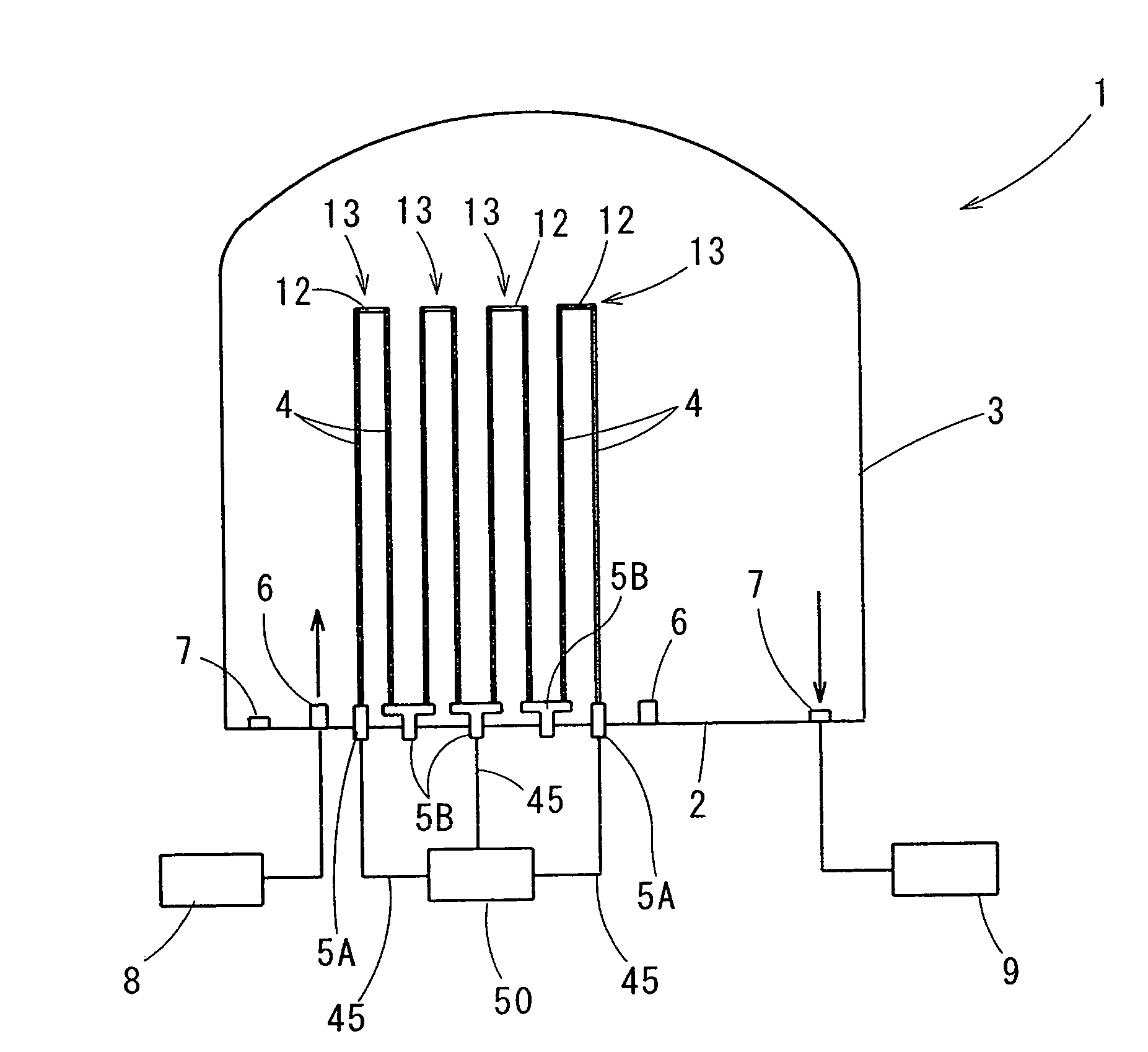
[0022]FIG. 3 is an overall view showing the polycrystalline silicon manufacturing apparatus according to a first embodiment of the present invention. A reaction furnace 1 of the polycrystalline silicon manufacturing apparatus includes a bottom plate portion 2 which forms a furnace bottom and a bell-shaped bell jar 3 which is detachably attached onto the bottom plate portion 2. In this case, an upper surface of the bottom plate portion 2 is in a substantially flat horizontal plane. The bell jar 3 is formed in a bell shape as a whole, and a ceiling is formed in a dome shape. Additionally, walls of the bottom plate portion 2 and the bell jar 3 are formed into a jacket structure and are cooled by cooling water.

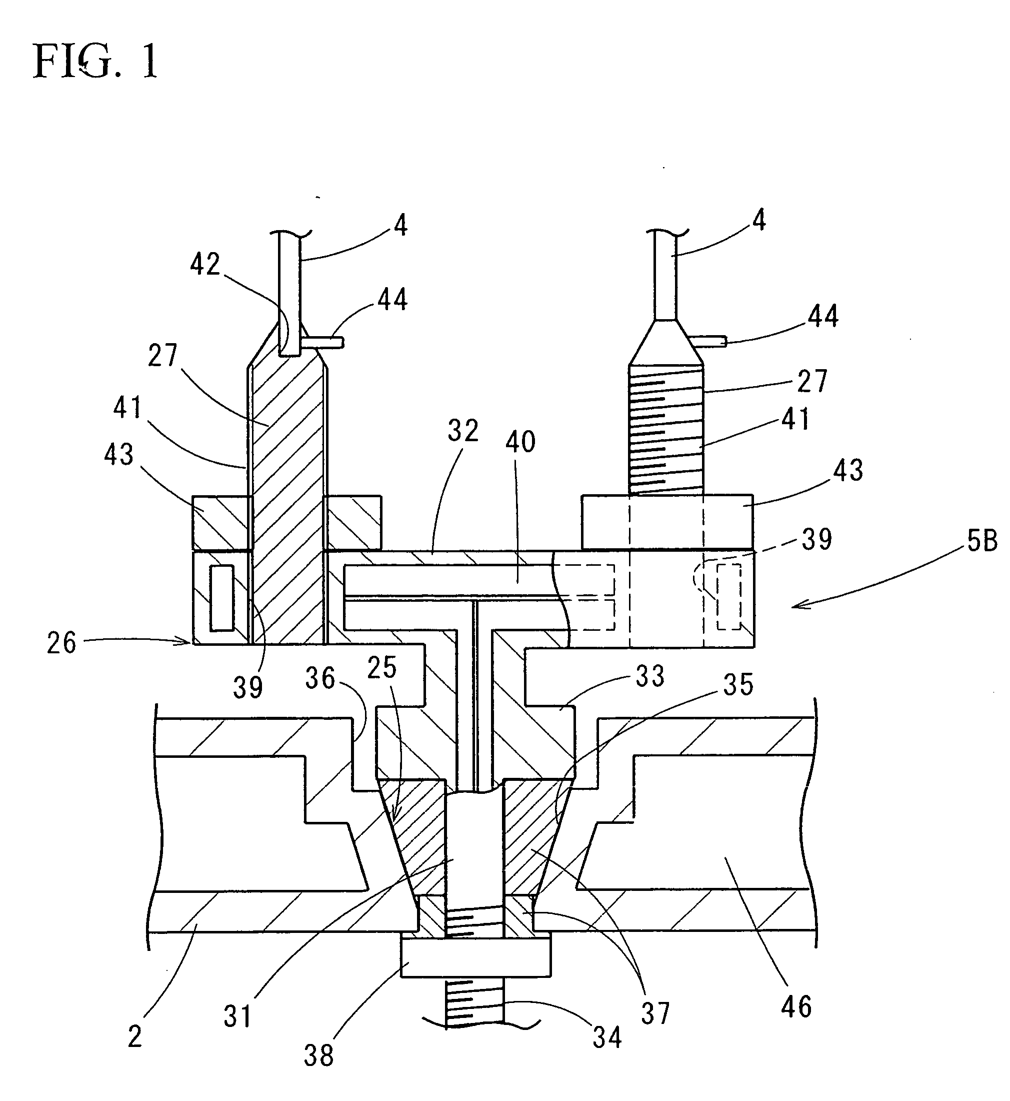
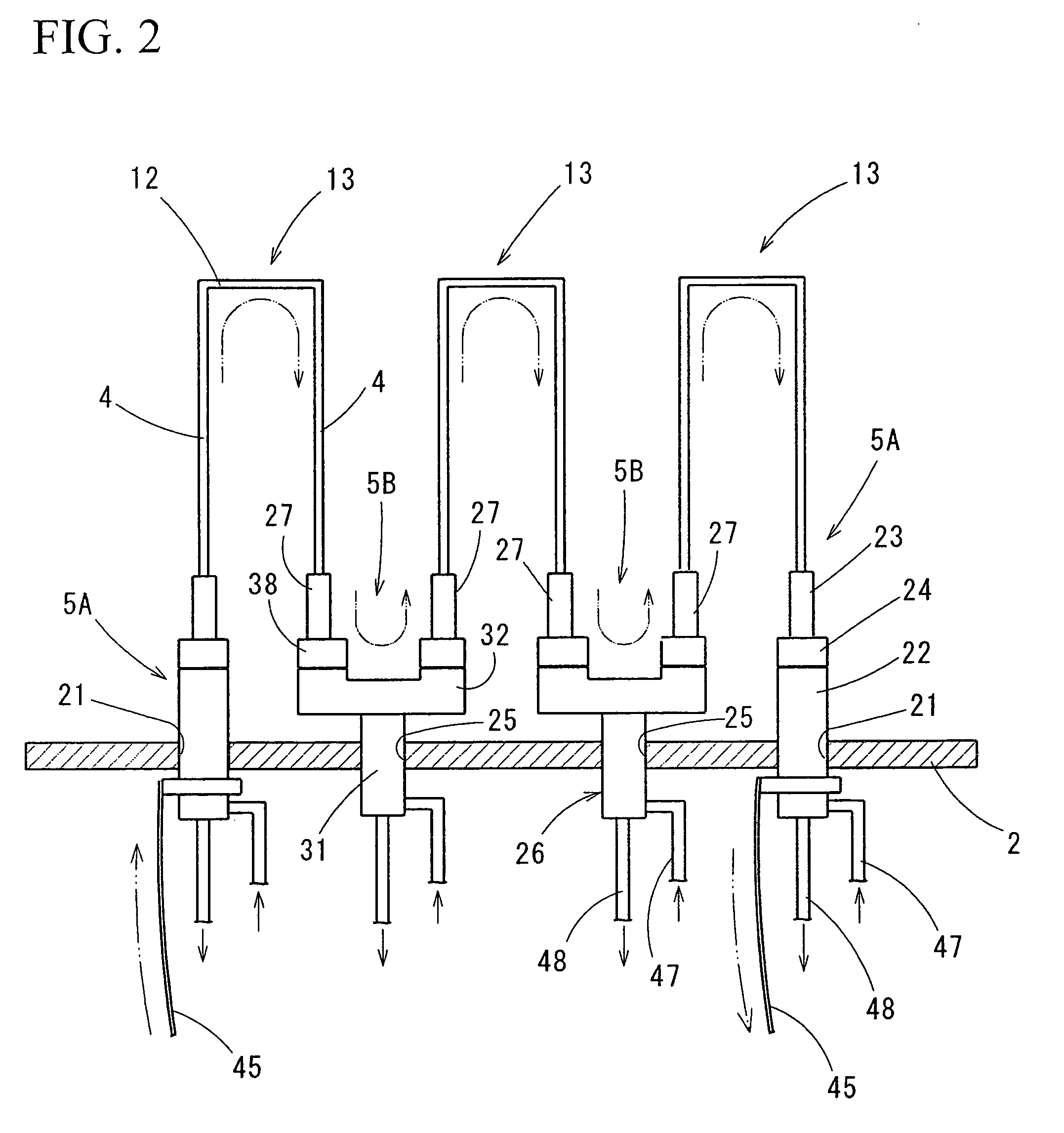
[0023]The bottom plate portion 2 is provided with plural electrodes 5A and 5B which are mounted with...


PUM

PropertyMeasurementUnit
currentaaaaaaaaaa
currentaaaaaaaaaa
resistanceaaaaaaaaaa

Abstract

A polycrystalline silicon manufacturing apparatus is provided which supplies raw gas to the inside of a reaction furnace and supplies a current from an electrode to a silicon seed rod in a state where the vertically extending silicon seed rod is uprightly stood on each of the plural electrodes disposed in a bottom plate portion of the reaction furnace so as to heat the silicon seed rod and thus to deposit polycrystalline silicon on a surface of the silicon seed rod by means of the reaction of the raw gas.

Description

BACKGROUND OF THE INVENTION[0001]1. Field of the Invention[0002]The present invention relates to a polycrystalline silicon manufacturing apparatus which manufactures a polycrystalline silicon rod by depositing polycrystalline silicon on a surface of a heated silicon seed rod.[0003]Priority is claimed on Japanese Patent Application No. 2008-084308, filed Mar. 27, 2008, the content of which is incorporated herein by reference.[0004]2. Description of the Related Art[0005]Conventionally, as this kind of polycrystalline silicon manufacturing apparatus, a polycrystalline silicon manufacturing apparatus using the Siemens method is known. In the polycrystalline silicon manufacturing apparatus using the Siemens method, plural seeds made of silicon are arranged in a hermetic reaction furnace and are heated, raw gas composed of a mixed gas of chlorosilane and hydrogen is supplied to the reaction furnace to contact with the heated silicon seed rods, and then deposit polycrystalline silicon on s...

Claims


Application Information

Patent Timeline
Patent Type & Authority Applications(United States)
IPC IPC(8): C23C16/24
CPCC01B33/035Y10T117/10Y10T117/102C23C16/4418
Inventor ENDOH, TOSHIHIDETEBAKARI, MASAYUKIISHII, TOSHIYUKISAKAGUCHI, MASAAKI
Owner HIGH-PURITY SILICON CORP
Why Eureka
Try Eureka