Display device

Inactive Publication Date: 2009-10-01
MITSUBISHI ELECTRIC CORP
View PDF0 Cites 10 Cited by
  • Summary
  • Abstract
  • Description
  • Claims
  • Application Information

AI Technical Summary

Benefits of technology

[0019]According to the invention, since it is possible to carry out the display inspection capable of performing an arbitrary display before the COG-mou

Problems solved by technology

When the pitch becomes narrow, a position deviation occurs between the mounting terminals of the substrate and the bump electrodes of the driving circuit chip, thereby causing a problem of a difficult electric connection.
In the former simple display inspection, several number of inspection terminals may be provided, but a precise inspection cannot be carried out.
In addition, in the case where a defective state occurs due to static electricity upon cutting each wiring and the common inspection terminal for each color so as to be separated after the display in

Method used


Image

  • Display device
  • Display device
  • Display device

Examples


Example

First Embodiment

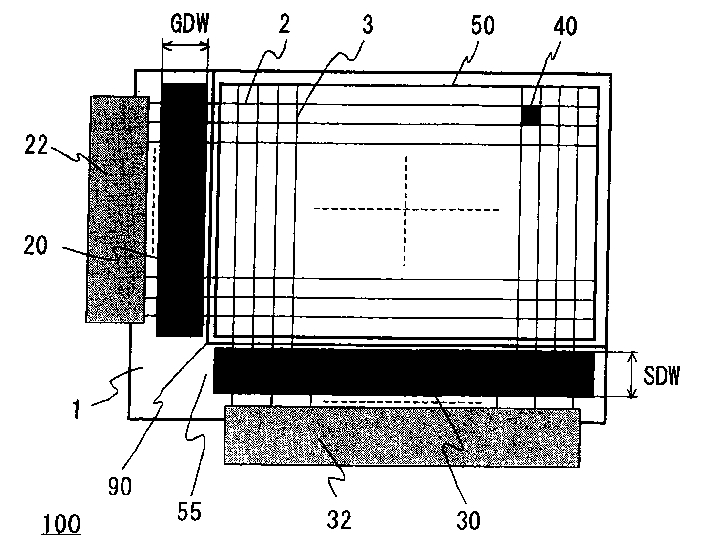
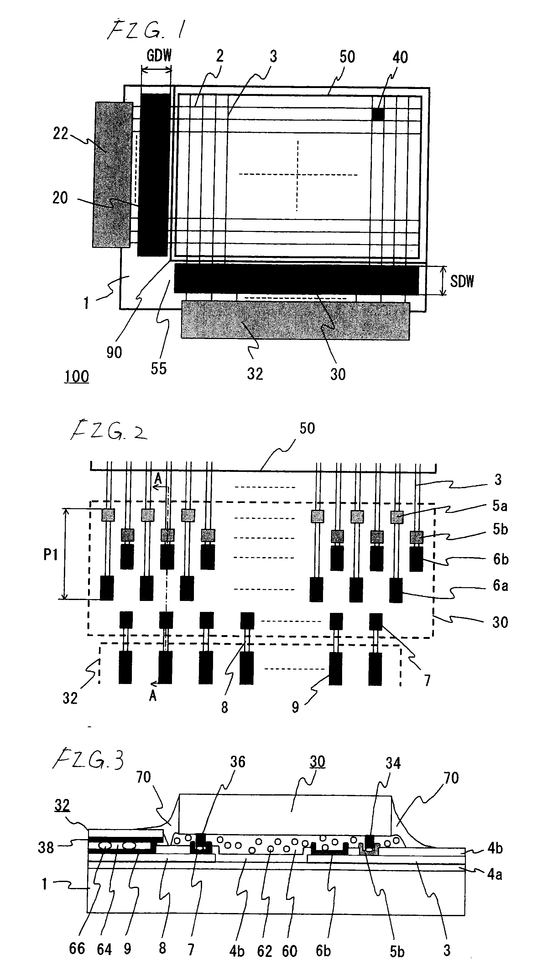
[0030]FIG. 1 is a top view showing a schematic configuration of a display device according to a first embodiment of the invention.

[0031]The display device shown in FIG. 1 is a liquid crystal display device 100. An array substrate 1 formed of transparent insulating material such as glass has thereon a display area 50 in which plural pixels 40 are arranged in a matrix shape. Each pixel 40 is formed in an area surrounded by gate wirings 2 and source wirings 3 and is formed by a TFT switch, a pixel electrode, a holding capacity, and the like (which are not shown in the drawing). Additionally, in a frame area 55 on the outside of the display area 50, the gate wirings 2 and the source wirings 3 used to drive the pixels 40 are drawn out and connected to a gate driving circuit chip 20 and a source driving circuit chip 30.

[0032]The gate driving circuit chip 20 and the source driving circuit chip 30 are directly COG-mounted on the array substrate 1. The output sides of the gat...

Example

Second Embodiment

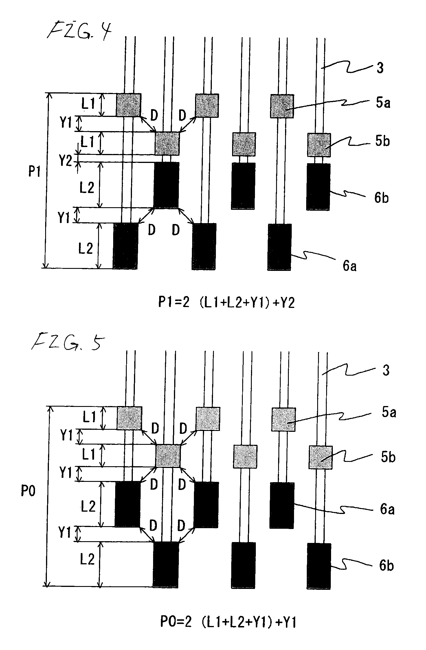
[0066]FIG. 6 is a top view magnifying an area of the source driving circuit chip of the display device according to a second embodiment of the invention. FIG. 7 is a top view further magnifying the output-side mounting terminals and the inspection terminals.

[0067]In the second embodiment, a gap Y1 between the output-side mounting terminal 5b and the inspection terminal 6b is set to “0”, and hence the output-side mounting terminal 5b and the inspection terminal 6b are formed into an integrated terminal 56. Accordingly, it is possible to allow an output-side-terminal-area length P2 to be much smaller than the terminal-area length P1 according to the first embodiment. Also, it is possible to cope with the additional narrow frame width of the width SDW of the source driving circuit chip 30.

[0068]In addition, as shown in FIG. 7, in the integrated terminal 56 according to the second embodiment, in order to indicate a boundary between the output-side mounting terminal 5b a...

Example

Third Embodiment

[0071]FIG. 8 is a top view further magnifying the area of the source driving circuit chip of the display device according to a third embodiment of the invention.

[0072]In the third embodiment, in the same manner as the second embodiment, the output-side mounting terminal 5b and the inspection terminal 6b are formed into the integrated terminal 56. Also, a length of the integrated terminal 56 is set to be smaller than “L1+L2” obtained by adding a length L1 of the output-side mounting terminal 5a to a length L2 of the inspection terminal 6a. Accordingly, it is possible to allow a terminal-area length P3 to be much smaller than those of the first and second embodiments. Also, it is possible to cope with the additional narrow frame width of the width SDW of the source driving circuit chip 30.

[0073]In FIG. 8, the length of the output-side mounting terminal 5b is smaller than that of the output-side mounting terminal 5a, but the length of the inspection terminal 6b may be s...


PUM


Abstract

An array substrate is provided with thereon a display area in which plural pixels are arranged in a matrix shape. Output-side mounting terminals for a source driving circuit chip, which is COG-mounted on a frame area on the outside of the display area, have a plural-row zigzag arrangement. Inspection terminals individually provided in correspondence to the output-side mounting terminals have a zigzag arrangement opposite to the zigzag arrangement of the output-side mounting terminals in a terminal-row direction. Additionally, the output-side mounting terminals and the inspection terminals are disposed below the source driving circuit chip.

Description

[0001]This application claims priority from Japanese Patent Application No. 2008-083311 filed on Mar. 27, 2008, the entire subject matter of which is incorporated herein by reference.BACKGROUND OF THE INVENTION[0002]1. Field of the Invention[0003]The present invention relates to a display device, and more particularly, to a configuration of mounting terminals and inspection terminals of a display device in which a driving circuit chip for driving pixels forming a display area is directly mounted onto an array substrate.[0004]2. Description of the Related Art[0005]In recent years, a display device has been used as information display means for an observer in various apparatuses. Currently, instead of a Braun tube which has been mainly used so far, a new thin-type display device has been introduced which uses liquid crystal, plasma, EL (Electro Luminescence), or FED (Field Emission Display). In particular, since a small-sized model or a large-sized model can be manufactured in a liqui...

Claims


Application Information

Patent Timeline
IPC IPC(8): G01R31/02
CPCG02F1/13452G09G3/006G09G3/3611G09G2300/0426
Inventor NOUMI, SHIGEAKIMASUTANI, YUICHI
Owner MITSUBISHI ELECTRIC CORP
Why Eureka
Try Eureka