Socket, test device and test method for testing electronic element packages with leads

a test method and electronic element technology, applied in the field of sockets, test devices and test methods for testing image sensors with leads, can solve the problems of increasing the cost of testing, reducing the test rate, and reducing so as to reduce the time of changing the probe, prevent the deflective placement and damage of the image sensor, and increase the lifetime of the prob

Inactive Publication Date: 2009-10-01
KING YUAN ELECTRONICS
View PDF8 Cites 21 Cited by
  • Summary
  • Abstract
  • Description
  • Claims
  • Application Information

AI Technical Summary

Benefits of technology

[0015]Therefore, the effect achieved with the present invention, that is not found in prior art, is to provide a socket, test device and a test method for testing the electronic element packages with leads or the image sensors with leads that capable of preventing the deflective placing and damage of the image sensor with leads. It can increase the lifetime of the probes and decrease the times of changing the probes for increases test rate. Furthermore, it can provide a shorter electronic signal delivering path and improving the accuracy and the reliability of the test process.

Problems solved by technology

It decreases the lifetime of the probes and increases the cost of the test, and furthermore, it decreases the test rate because the probes need to be changed more frequently.
Besides, the test device or the socket, as showed in FIG. 1A, can not be used for testing an image sensor.
However, the test device or the socket showed in FIG. 1A can not be used for testing the image sensor with leads, and the image sensor with leads are tested by the test device or the socket showed in FIG. 2 for the image sensor without leads.
This signal delivering path is too long and need to pass through too many elements so that the contacting capacity increases and the accuracy and the reliability of the test decrease.

Method used


Image

  • Socket, test device and test method for testing electronic element packages with leads
  • Socket, test device and test method for testing electronic element packages with leads
  • Socket, test device and test method for testing electronic element packages with leads

Examples


Embodiment Construction

[0025]The following is the detailed description of the embodiments of the present invention. It is appreciated that the processes and structures described below do not entirely encompass whole processes and structures. The present invention could be practiced in conjunction with various fabrication techniques, and only the commonly practiced processes are included to provide an understanding of the present invention.

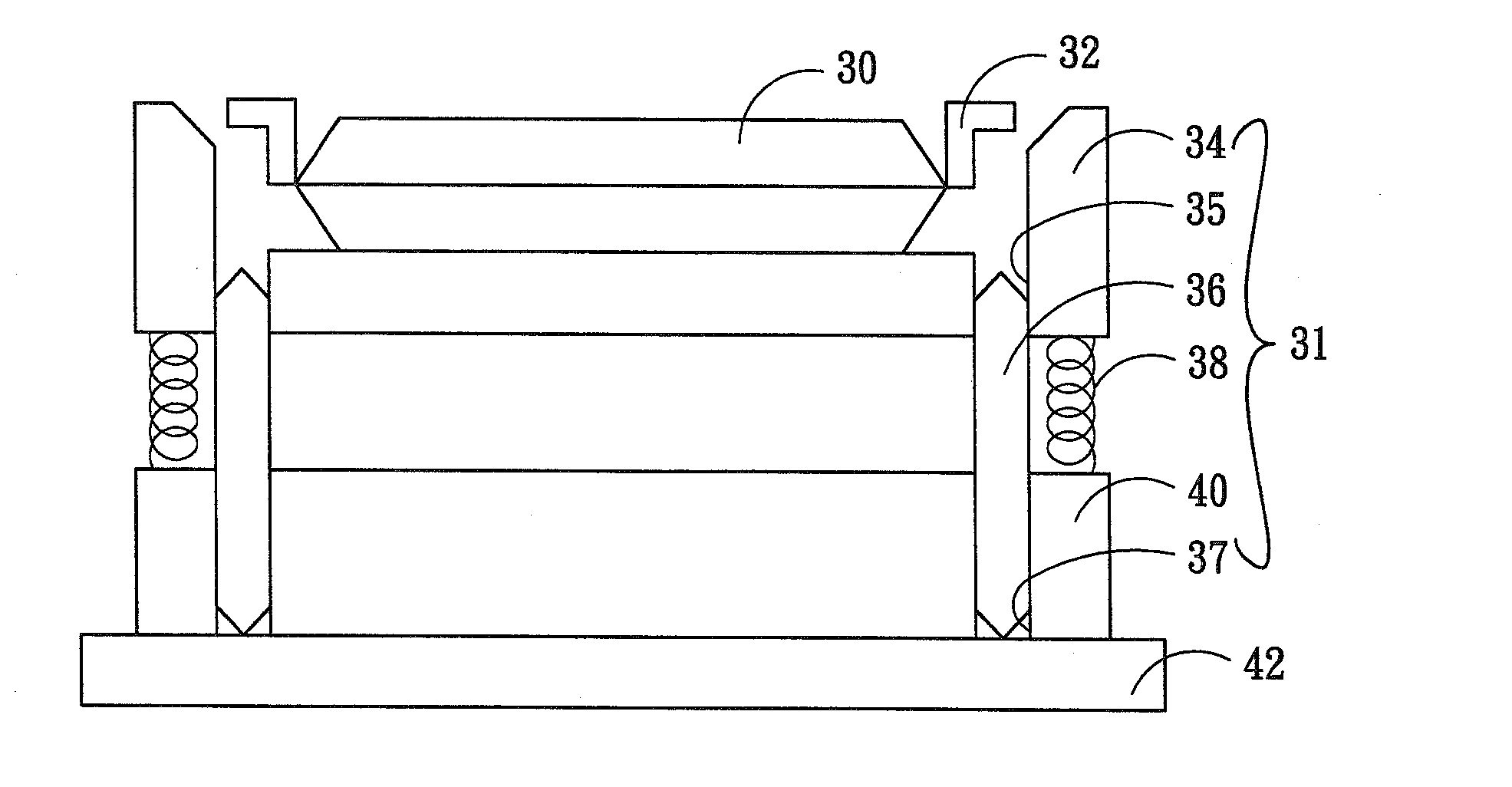
[0026]Referring to FIG. 3A, it is a cross-sectional view illustrating a test device for testing the electronic element packages with leads according to one embodiment of the present invention. The test device comprises a socket 31, a plurality of test probes 36 and a test circuit board 42. The socket 31 comprises a base 40 having a plurality of first holes 37, a guiding structure 34 that is used for guiding and holding a electronic element package 30 with leads to be tested has a plurality of second holes 35 (FIG. 3A is a plane view illustrating the guiding structure 34)...


PUM


Abstract

The present invention relates to a socket, test device and test method for testing electronic element packages with leads, and particularly relates to a socket, test device and test method for testing image sensors with leads. The test device comprises a socket, a plurality of test probes and a test circuit board. The socket comprises a base having a plurality of first holes, a guiding structure having a plurality of second holes and at least one floating member used to connect the base and the guiding structure. In the socket, test device and test method of the present invention, each test probe is received into one first hole and one second hole to maintain the top surface of guiding structure to be even for preventing the deflective placing of the electronic element packages, and for preventing the damage to the test probes. The test probes are controlled by compressing the floating member for protruding form the top surface of the guiding structure and for providing a shorter delivering path of the electronic signals between the test circuit board and the electronic element packages. This shorter delivering path of the electronic signals can improve the accuracy and reliability of the test process for the electronic element packages with leads.

Description

BACKGROUND OF THE INVENTION[0001]1. Field of the Invention[0002]A socket, test device and test method for testing electronic element packages with leads, and particularly relates to a socket, test device and test method for testing image sensors with leads.[0003]2. Description of the Prior Art[0004]After the manufacturing process of electronic elements is finished, a circuit probe test is performed to recognize and confirm the quality of the electronic elements for preparing to package the electronic elements. It prevents from the waste of the packaging process which is resulted from packaging the electronic elements with bad quality. Furthermore, a final test is performed to recognize and confirm the packaged electronic elements without any damage and in scale.[0005]A test device and test method for the common packaged electronic elements with leads, for example Quad Flat Package (QFP), is illustrated in FIG. 1A. Referring to FIG. 1A, an electronic element package 10 is placed in a...

Claims


Application Information

Patent Timeline
Patent Type & Authority Applications(United States)
IPC IPC(8): G01R31/28
CPCG01J1/04G01R1/0466G01J1/08G01J1/0403
Inventor CHANG, CHIU-FANG
Owner KING YUAN ELECTRONICS
Why Eureka
Try Eureka