Hybrid superconducting-magnetic memory cell and array

a superconducting and magnetic memory technology, applied in the field of hybrid magnetic memory including magnetoresistive elements and superconducting elements, can solve the problems of wasting the processor's potential computational power, discharging a great deal of power, and unable to meet the needs of high-capacity, high-capacity random access memory,

Active Publication Date: 2009-10-01
IBM CORP
View PDF6 Cites 28 Cited by
  • Summary
  • Abstract
  • Description
  • Claims
  • Application Information

AI Technical Summary

Problems solved by technology

The development of superconducting technology for general-purpose computing applications, however, has been largely impeded by the lack of dense, fast, and high capacity (i.e., high bit count) random access memory (RAM).
Without a high capacity and low access-time memory to feed it data, a processor (especially a processor operating at the clock rates supported by superconducting logic) would be continually star

Method used


Image

  • Hybrid superconducting-magnetic memory cell and array
  • Hybrid superconducting-magnetic memory cell and array
  • Hybrid superconducting-magnetic memory cell and array

Examples


first embodiment

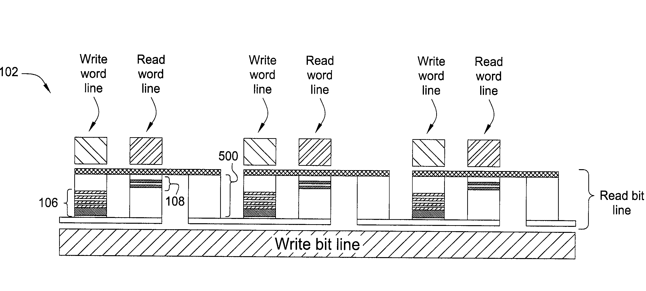
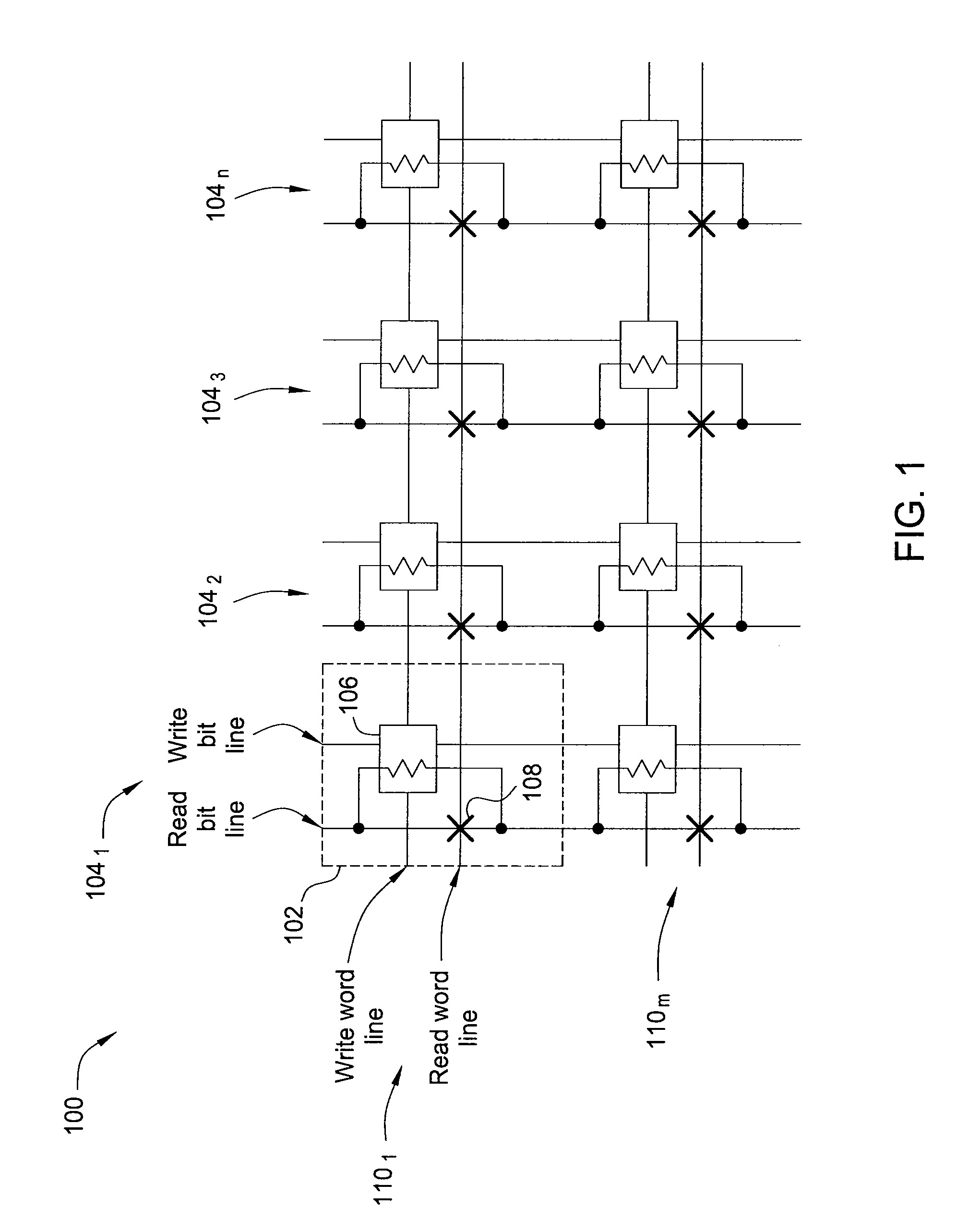
[0016]FIG. 1 is a schematic diagram illustrating a magnetic random access memory (MRAM) array 100, according to the present invention. In one embodiment, the MRAM array 100 is a two-dimensional array.

[0017]As illustrated, the MRAM array 100 comprises a plurality of memory cells, an exemplary one of which is designated as memory cell 102. As illustrated, a first plurality of these memory cells is wired in series along the read bit line to form one column of the MRAM array 100 (see, e.g., exemplary column 1041). Two or more of these columns 1041-104n (hereinafter collectively referred to as “columns 104”) are then positioned adjacent to each other, along with appropriate write word lines and read word lines along each resultant row 1101-110m (hereinafter collectively referred to as “rows 110”), to form the two-dimensional MRAM array 100.

[0018]In one embodiment, each memory cell in the MRAM array 100 is configured in accordance with the exemplary memory cell 102. Thus, each memory cell...

second embodiment

[0034]FIG. 7 is a schematic diagram illustrating an MRAM array 700, according to the present invention. In one embodiment, the MRAM array 700 is a two-dimensional array.

[0035]As illustrated, the MRAM array 700 is configured in a manner substantially similar to the MRAM array 100 illustrated in FIG. 1 and comprises a plurality of memory cells, an exemplary one of which is designated as memory cell 702. As illustrated, a first plurality of these memory cells is wired in series along the read bit line to form one column of the MRAM array 700 (see, e.g., exemplary column 7041). Two or more of these columns 7041-704n (hereinafter collectively referred to as “columns 704”) are then positioned adjacent to each other, along with appropriate write word lines and read word lines along each resultant row 7101-710m (hereinafter collectively referred to as “rows 710”), to form the two-dimensional MRAM array 700.

[0036]In one embodiment, each memory cell in the MRAM array 700 is configured in acco...


PUM


Abstract

In one embodiment, the invention is a hybrid superconducting-magnetic memory cell and array. One embodiment of a memory cell includes a magnetoresistive element and at least one superconducting element wired in parallel with the magnetoresistive element. In a further embodiment, memory cells of the disclosed configuration are arranged to form a memory array.

Description

BACKGROUND OF THE INVENTION[0001]The present invention relates generally to magnetic memory, and more specifically relates to hybrid magnetic memory including a magnetoresistive element and a superconducting element.[0002]Superconducting technology such as that based on Josephson junctions has long seemed promising for implementing high-performance computer systems due to: (1) the very fast switching of superconducting elements; and (2) the low power dissipation of superconducting elements relative to semiconductor circuits (e.g., complementary metal-oxide-semiconductor (CMOS)).[0003]The development of superconducting technology for general-purpose computing applications, however, has been largely impeded by the lack of dense, fast, and high capacity (i.e., high bit count) random access memory (RAM). Without a high capacity and low access-time memory to feed it data, a processor (especially a processor operating at the clock rates supported by superconducting logic) would be continu...

Claims


Application Information

Patent Timeline
IPC IPC(8): G11C11/02G11C11/44G11C11/416G11C7/00
CPCG11C8/14G11C11/15H01L27/18G11C11/161H01L39/16H01L39/223H01L43/08H01L27/222G11C11/44G11C11/1673G11C11/1657G11C11/1675G11C11/1659G11C11/1655H10B61/10H10N69/00H10B61/00H10N50/10H10N60/12H10N60/30
Inventor BULZACCHELLI, JOHN F.GALLAGHER, WILLIAM J.KETCHEN, MARK B.
Owner IBM CORP
Why Eureka
Try Eureka