
Semiconductor circuit design method and semiconductor circuit manufacturing method

a semiconductor circuit and circuit technology, applied in the field of semiconductor circuit manufacturing methods and semiconductor circuit design methods, can solve the problem that the technology given above has no contrivance for optimizing the actual circuit, and achieve the effect of optimizing the circuit and efficiently acquiring the layout of the semiconductor circui

Inactive Publication Date: 2009-10-01
SOCIONEXT INC
View PDF8 Cites 15 Cited by
  • Summary
  • Abstract
  • Description
  • Claims
  • Application Information

AI Technical Summary

Benefits of technology

[0005]The technologies given above have no contrivance for optimizing the actual circuit including the multiplicity of elements. According to an aspect of the embodiment, there is proposed a technology that can be applied to a design of a semiconductor circuit including the multiplicity of elements. The present technology is capable of efficiently acquiring a layout of the semiconductor circuit that conforms with desired circuit characteristics, and manufacturing an optimized circuit.

Problems solved by technology

The technologies given above have no contrivance for optimizing the actual circuit including the multiplicity of elements.

Method used


Image

  • Semiconductor circuit design method and semiconductor circuit manufacturing method
  • Semiconductor circuit design method and semiconductor circuit manufacturing method
  • Semiconductor circuit design method and semiconductor circuit manufacturing method

Examples


Embodiment Construction

)

[0033]Preferred embodiments of the present invention will hereinafter be explained with reference to accompanying drawings. As the embodiments, a technology of a computer aided design equipment, a computer aided design method and semiconductor circuit manufacturing method will hereinafter be described. Configurations in the following embodiments are exemplifications, and the present invention is not limited to the configurations in the embodiments.

[0034]According to the technology, the layout of the semiconductor circuit, which conforms with the desired circuit characteristics, can be efficiently acquired.

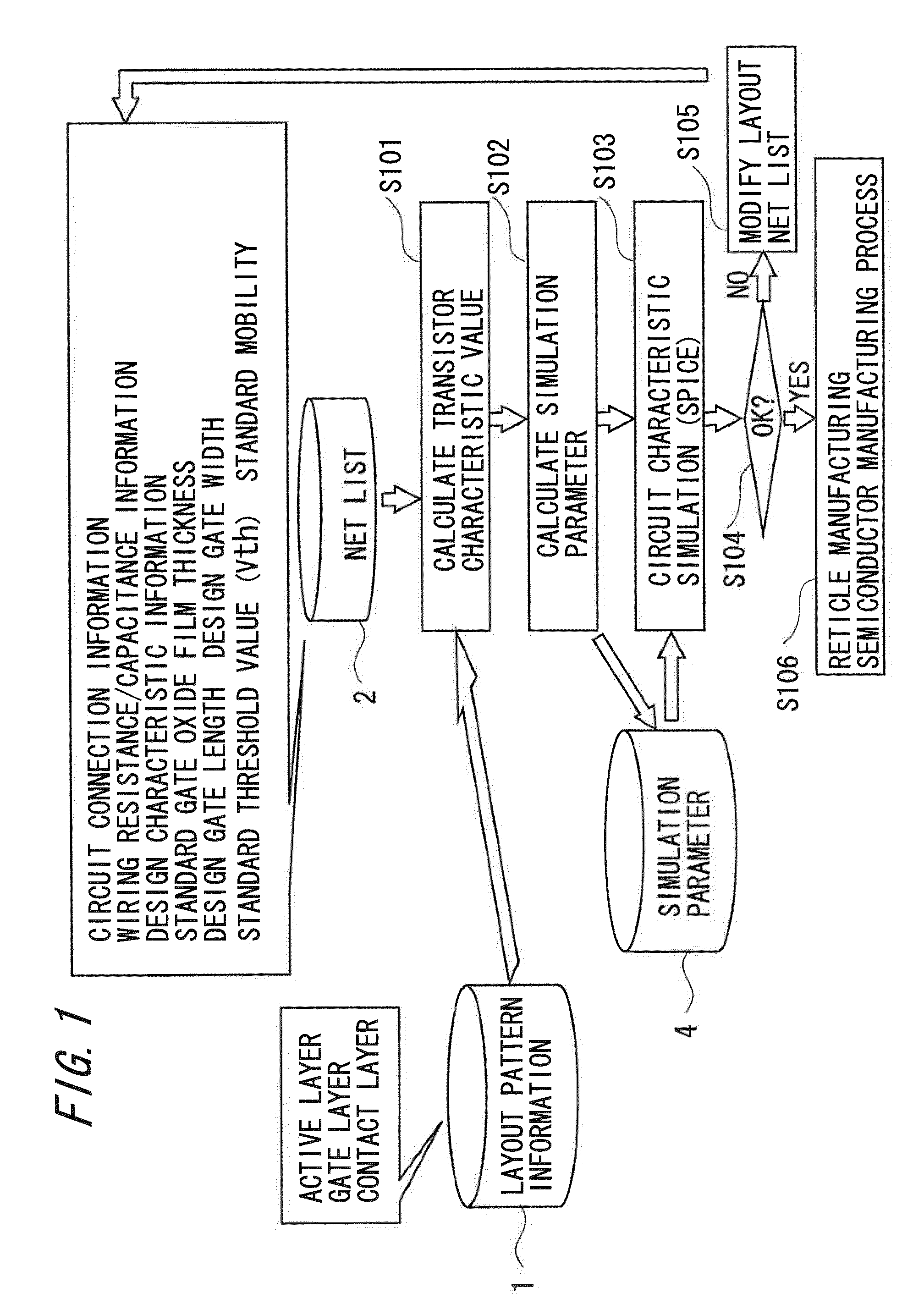
[0035]FIG. 1 illustrates an outline of a semiconductor manufacturing process according to the embodiment. In the semiconductor manufacturing process, S101 through S105 are steps related to a design of a semiconductor device, and S106 is a step related to manufacture of the semiconductor device.

[0036]A semiconductor circuit generally includes a multiplicity of transistors. The semi...


PUM


Abstract

A computer converts dimensions of design patterns of components of the transistors configuring the semiconductor circuit or component parameters extracted from in-design physical characteristics of the transistors into simulation parameters inputted to the simulator, organize the plurality of transistors included in the semiconductor circuit into a plurality of groups, selects any selection groups from the plurality of groups, sets fixed parameter values as component parameters of the non-selected groups other than the selection groups in the plurality of groups, sets the combinations of the component parameters in the selection groups, acquires circuit characteristics with respect to each combination of the component parameters, selects a group as a next selection group different from the selected groups, and repeatedly executing the setting the fixed parameter values through the selects a group as a next selection group different.

Description

CROSS-REFERENCE TO RELATED APPLICATIONS[0001]This application is based upon and claims the benefit of priority of the prior Japanese Patent Application No. JP2008-086738, filed on Mar. 28, 2008, the entire contents of which are incorporated herein by reference.FIELD[0002]The embodiment(s) discussed herein is (are) related to a semiconductor circuit design method and a semiconductor circuit manufacturing method.BACKGROUND[0003]Over the recent years, with advanced micronization of LSI, circuit characteristics have been greatly influenced by accuracy of physical quantities of shapes of layout patterns, layout positions, etc of circuit elements, or scatters in these physical quantities in a manufacturing process. Further, there has been proposed a method of taking the influence thereof into a prediction of the circuit characteristics and optimizing the circuit characteristics.[0004]Conventional technologies are not, however, sufficient for optimizing the circuit characteristics of a who...

Claims


Application Information

Patent Timeline
Patent Type & Authority Applications(United States)
IPC IPC(8): G06F17/50
CPCG06F17/5036G06F30/367
Inventor ARIMOTO, HIROSHI
Owner SOCIONEXT INC
Learn More