Driver circuit for a display device, and driver cell

a technology of driver circuit and display device, which is applied in the direction of electric digital data processing, instruments, computing, etc., can solve the problems of non-uniform output characteristics of channels and adversely affect the signal output from circuit groups

Inactive Publication Date: 2012-10-04
LAPIS SEMICON CO LTD
View PDF10 Cites 7 Cited by
  • Summary
  • Abstract
  • Description
  • Claims
  • Application Information

AI Technical Summary

Benefits of technology

[0017]The novel driver cell provides extra space for the large output transistors in the operational amplifier and permits a space efficient layout of driver cells.

Problems solved by technology

A problem with the arrangement shown in FIG. 2 is that since the length of the metal wiring patterns connecting the operational amplifiers to the output pads differs from channel to channel, the output characteristics of the channels are non-uniform.
A particular problem is that the wiring resistance in the long metal wiring patterns 17A adversely affects the slew rate of the signals output from circuit group A.

Method used


Image

  • Driver circuit for a display device, and driver cell
  • Driver circuit for a display device, and driver cell
  • Driver circuit for a display device, and driver cell

Examples


Embodiment Construction

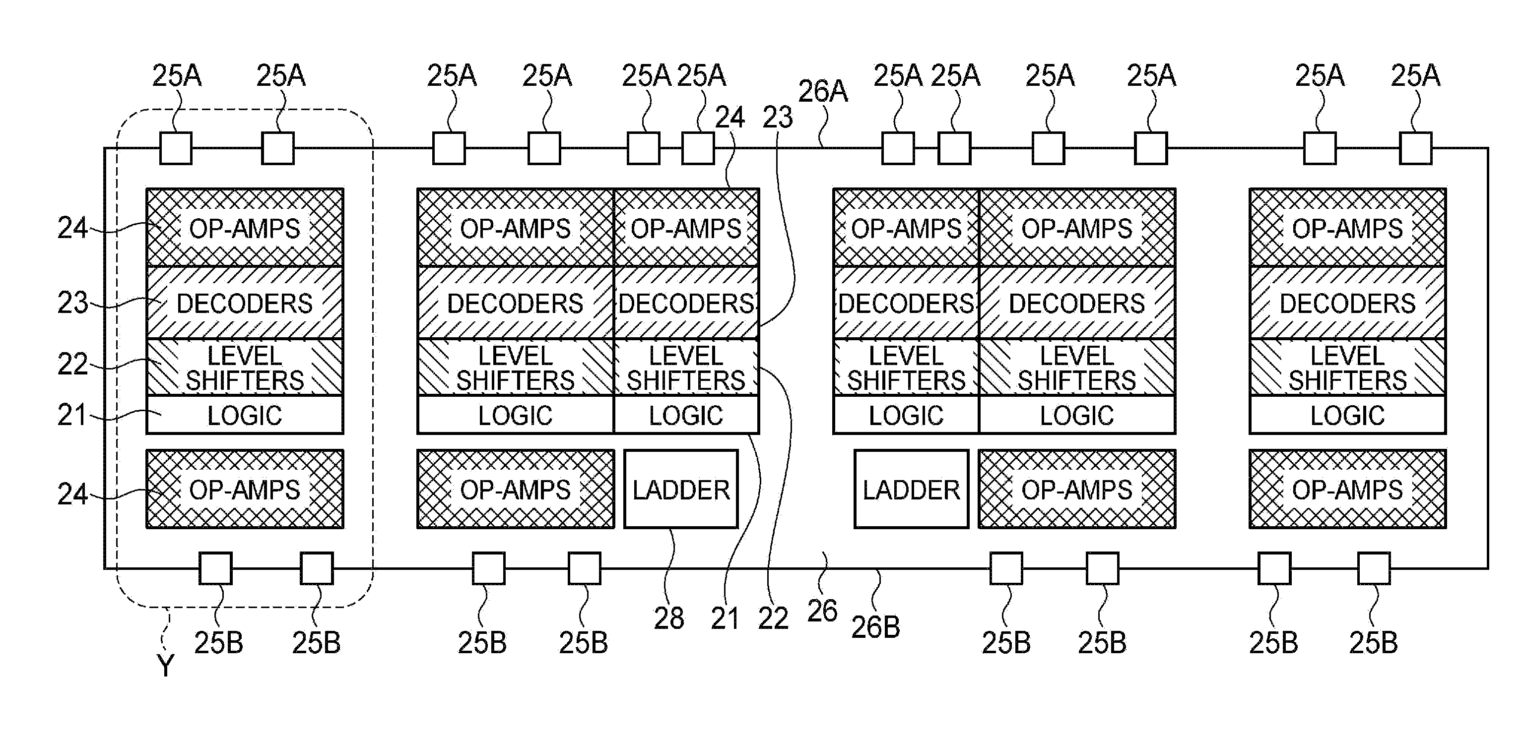
[0025]Novel driver circuits will now be described with reference to FIGS. 3 to 6, in which like elements are indicated by like reference characters.

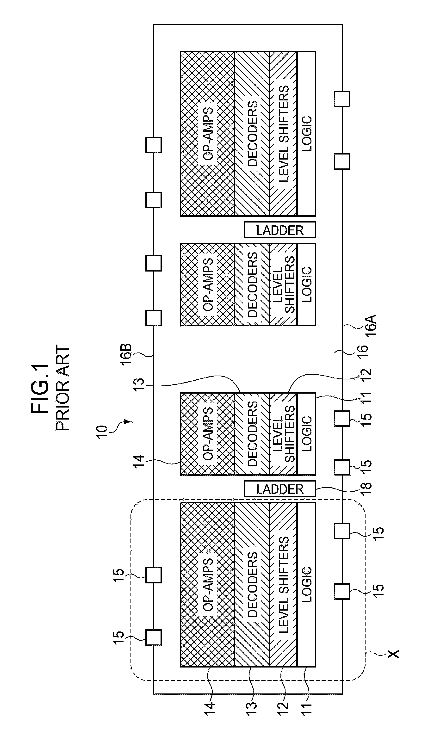
[0026]Referring to FIG. 3, an exemplary novel driver circuit includes logic circuits 21, level shifters 23, decoders 23, operational amplifiers 24, and output pads 25A, 25B formed on a rectangular semiconductor chip substrate 26 having two long sides 26A, 26B. Output pads 25A are disposed on the first long side 26A. Output pads 25B are disposed on the second long side 26B. A difference between this driver circuit and the conventional driver circuit 10 in FIG. 1 is that the operational amplifiers 24 are formed adjacent both long sides 26A, 26B.

[0027]The driver circuit also includes ladders 28 that supply selectable voltage signals representing possible pixel gradations on the display panel (not shown) driven by the driver circuit. The display panel may be, for example, a liquid crystal display panel. Each ladder 28 may be configured as a ...


PUM


Abstract

A driver circuit for driving a display panel is formed on a substrate and is organized into two families of sections. Each section includes a logic circuit, a level shifter, a decoder, an operational amplifier, and an output pad. In the first family, each section is laid out in the stated sequence (logic circuit, level shifter, decoder, operational amplifier, output pad). In the second family, each section is laid out in a different sequence: output pad, operational amplifier, logic circuit, level shifter, decoder. The output pads in the two families of sections are located on opposite sides of the substrate, and every output pad is adjacent to the operational amplifier to which it is connected. This arrangement reduces signal-to-signal variations in the output characteristics of the driver circuit and improves the slew rate of the output signals.

Description

BACKGROUND OF THE INVENTION[0001]1. Field of the Invention[0002]The present invention relates to a driver circuit and driver cell for a display device.[0003]2. Description of the Related Art[0004]A driver circuit for a display device is generally formed as an integrated circuit chip. The chip is sometimes referred to as a source driver because it is connected to the source terminals of transistors in the display panel of the display device.[0005]FIG. 1 shows a conventional source driver chip 10. The chip includes logic circuits 11, level shifters 13, decoders 13, operational amplifiers (OP-AMPs) 14, output pads 15, and one or more ladders 18 formed on a rectangular chip substrate 16. Responsive to input of an image data signal, the logic circuits 11, level shifters 13, decoders 13, and operational amplifiers 14 select voltages generated by the ladders 18 to generate voltage signals representing the gradation levels of pixels in the image.[0006]The logic circuits 11, level shifters 1...

Claims


Application Information

Patent Timeline
Patent Type & Authority Applications(United States)
IPC IPC(8): G09G5/10
CPCG09G3/20G09G3/3685G09G2320/0233G09G2310/027G09G2320/0223G09G2300/0426
Inventor IKARI, JUNKOHASEGAWA, HIDEAKI
Owner LAPIS SEMICON CO LTD
Why Eureka
Try Eureka