Partially captured oriented interconnections for BGA packages and a method of forming the interconnections

a technology of interconnections and bga packages, which is applied in the field of ball grid arrays, can solve the problems of increasing the compliance of solder joints, increasing the fatigue life of bga packages, and fatigue failure of bga interconnections, etc., and achieves sufficient wiring space, increased fatigue life, and enhanced pad adhesion

Inactive Publication Date: 2005-07-05
IBM CORP
View PDF21 Cites 128 Cited by
  • Summary
  • Abstract
  • Description
  • Claims
  • Application Information

AI Technical Summary

Benefits of technology

[0007]The present invention provides an integrated chip package, e.g., a BGA package, having an increased fatigue life, enhanced pad adhesion, while maintaining sufficient wiring space. In particular, the present invention provides a method of forming an integrated chip package having solder joints that are mask-defined in a first direction and pad-defined in a second direction.

Problems solved by technology

In the manufacture of BGA packages, thermal mismatch between the chip module and the printed circuit board may produce fatigue failure of the BGA interconnections, or solder joints.
One solution for this problem is the elongation of the solder joints, which increases the compliance of the solder joints, thereby increasing the fatigue life of the BGA package.
Unfortunately, stress concentrations within mask-defined solder joints tends to decrease the fatigue life of the solder joints.
However, many of these techniques reduce the amount of space on the printed circuit board available for wiring.

Method used


Image

  • Partially captured oriented interconnections for BGA packages and a method of forming the interconnections
  • Partially captured oriented interconnections for BGA packages and a method of forming the interconnections
  • Partially captured oriented interconnections for BGA packages and a method of forming the interconnections

Examples


Embodiment Construction

[0026]Although certain preferred embodiments of the present invention will be shown and described in detail, it should be understood that various changes and modifications may be made without departing from the scope of the appended claims. The scope of the present invention will in no way be limited to the number of constituting components, the materials thereof, the shapes thereof, the relative arrangement thereof, etc., and are disclosed simply as an example of the preferred embodiment. Although the drawings are intended to illustrate the present invention, the drawings are not necessarily drawn to scale.

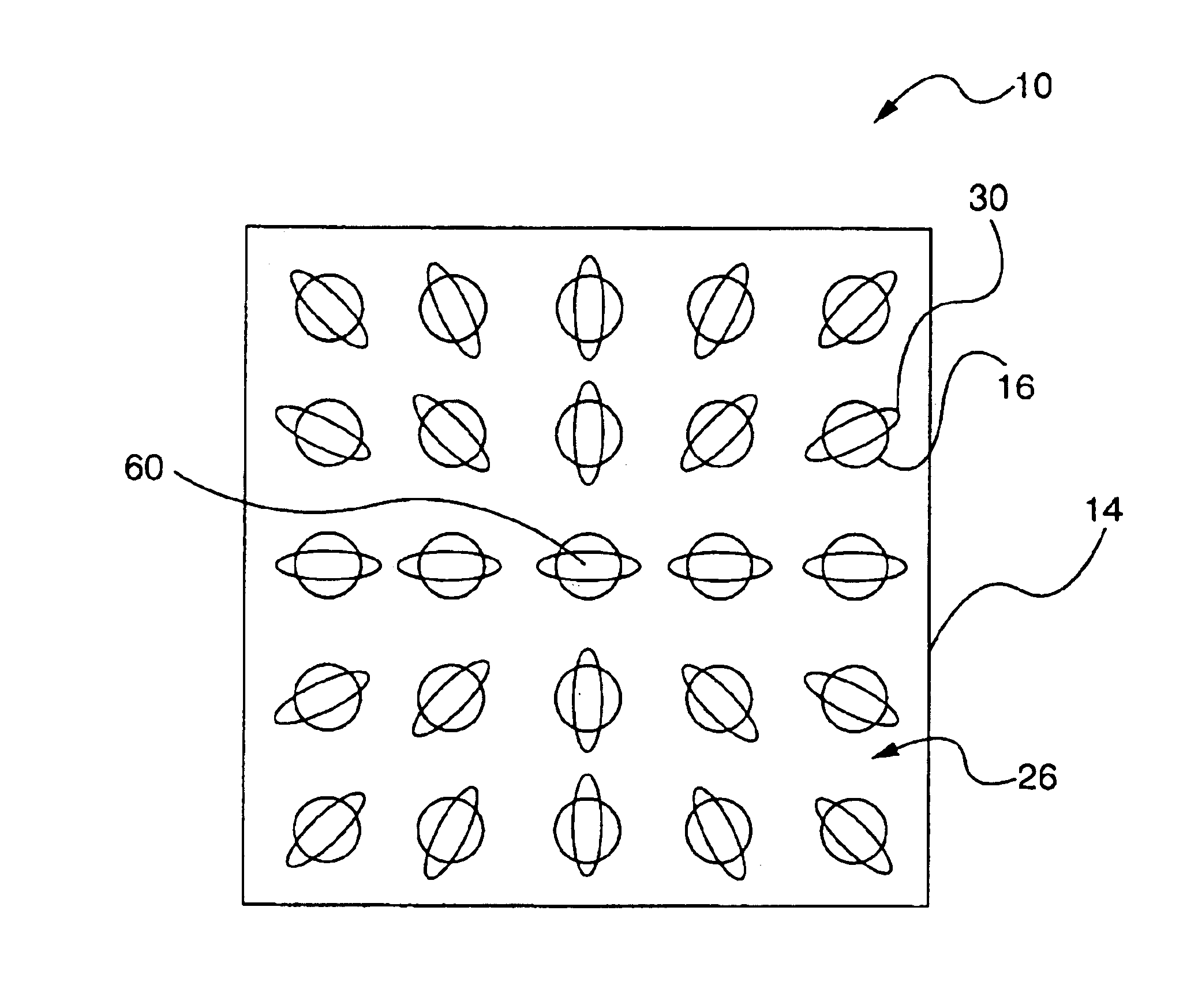
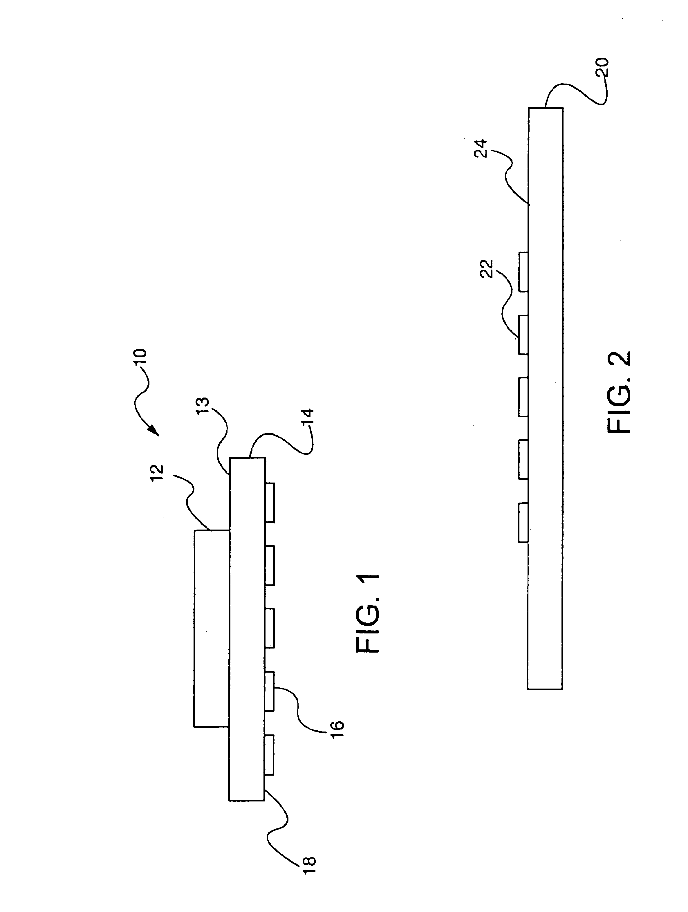
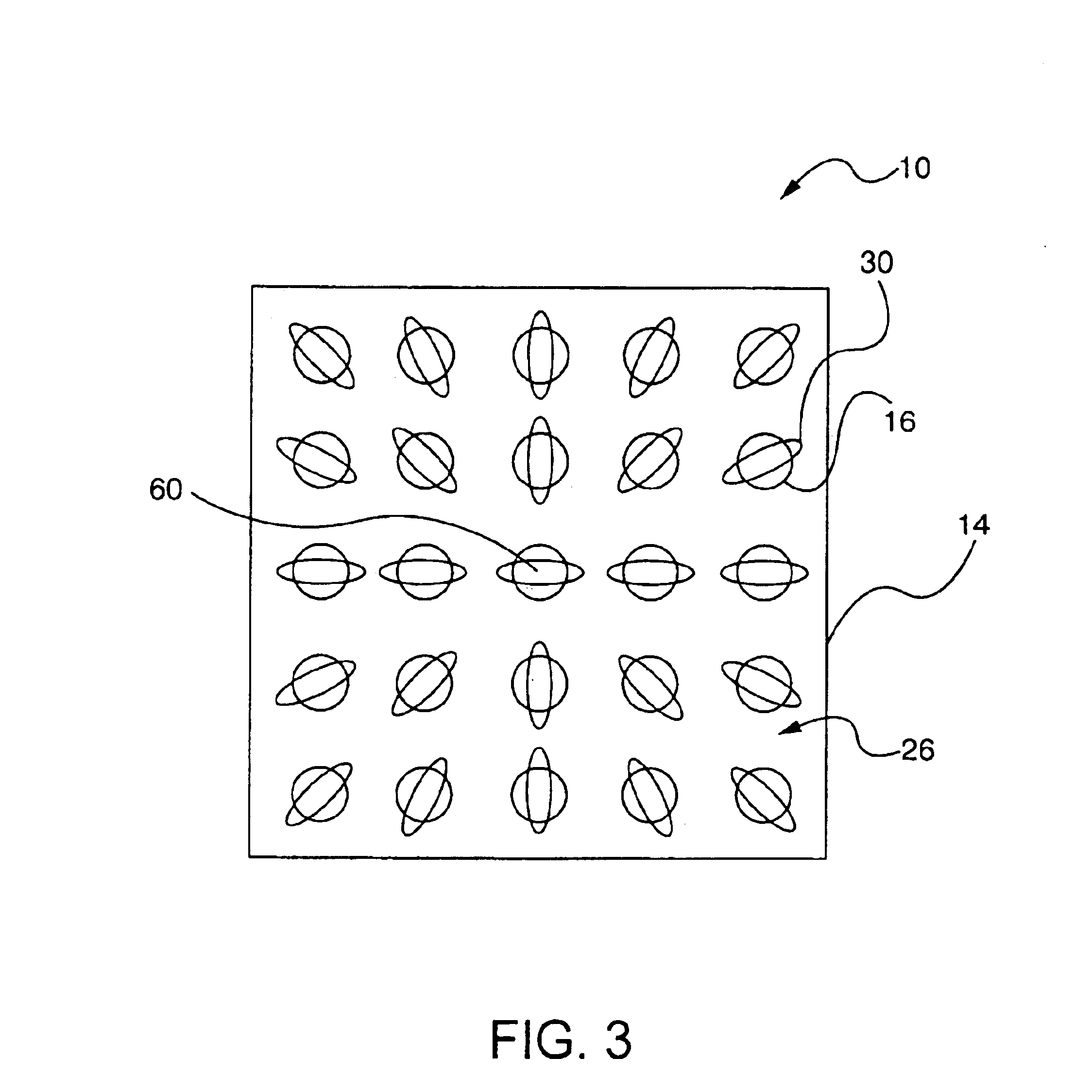
[0027]Referring to the drawings, FIG. 1 shows a semiconductor chip module 10 having an integrated circuit chip 12 electrically and mechanically connected to a first surface 13 of a chip carrier 14. The chip carrier 14 is made of an insulative non-wettable material, such as ceramic, FR4, IBM's Dry-Clad™, LCP (Liquid Crystal Polymer) polyimide, etc. A plurality of circular conducti...


PUM


Abstract

A Ball Grid Array package having an increased fatigue life and improved conductive pad adhesion strength, as well as providing sufficient wiring space within the package, is disclosed. In particular, solder joints having a combination of mask-defined and pad-defined solder joint profiles are formed using a mask having non-circular elongated openings. The non-circular elongated openings of the mask have a major axis and a minor axis, such that the dimension of the openings along the major axis is greater than the diameter of the conductive pads, and the dimension of the openings along the minor axis is less than the diameter of the conductive pads. In addition, the major axis of the openings within the mask are selectively oriented in the direction of highest stress for each solder joint within the package, while providing ample wiring space therein.

Description

[0001]This application is a divisional of Ser. No. 09 / 438,037; filed on Nov. 10, 1999 now U.S. Pat. No. 6,774,474.BACKGROUND OF THE INVENTION[0002]1. Technical Field[0003]The present invention relates generally to Ball Grid Array (hereinafter “BGA”) packages. In particular, the present invention relates to the use of partially captured interconnections, wherein the uncaptured region is selectively oriented in the direction of the highest stress within the BGA package.[0004]2. Related Art[0005]In the manufacture of BGA packages, thermal mismatch between the chip module and the printed circuit board may produce fatigue failure of the BGA interconnections, or solder joints. One solution for this problem is the elongation of the solder joints, which increases the compliance of the solder joints, thereby increasing the fatigue life of the BGA package. Solder joints have been elongated by the use of “captured pads” which form mask-defined solder joints. Along with increasing the height of...

Claims


Application Information

Patent Timeline
Patent Type & Authority Patents(United States)
IPC IPC(8): H01L23/50H01L23/28H01L23/31H01L23/498H01L23/48H05K3/34
CPCH01L23/3128H01L23/49816H01L23/50H05K3/3452H01L2924/15311H05K3/3436H05K2201/0989H05K2201/099H05K2201/10734H01L2924/00013H01L2224/29099H01L2924/0002H01L2924/00
Inventor CALETKA, DAVID V.JOHNSON, ERIC A.
Owner IBM CORP
Why Eureka
Try Eureka