Structure, materials, and methods for socketable ball grid

a socketable ball and grid technology, applied in the direction of manufacturing tools, sustainable manufacturing/processing, final product manufacturing, etc., can solve the problems of difficulty in visual inspection of solder joints, and difficulty in testing the bga assembly without damage to the soft solder bga, etc., to avoid thermal cycling induced failures, stable bga joint structure, and easy demountability

Inactive Publication Date: 2001-10-09
IBM CORP
View PDF46 Cites 42 Cited by
  • Summary
  • Abstract
  • Description
  • Claims
  • Application Information

AI Technical Summary

Benefits of technology

In view of the above, it seems desirable to modify the BGA structure to alleviate the thermal cycling induced failures at the module / ball interface and further provide a structure that is amenable to easy demounting so that module upgrade as well as testing and burn-in of BGA modules can be accomplished with ease and reliability. The present invention relates to a socketable ball grid array (SBGA) scheme that makes the above possible. In accordance with the present invention, a strong and compliant interconnection of BGA spheres to ceramic or plastic substrates is made possible. Moreover, the present invention makes it possible to provide a stable BGA joint structure which does not cause an excessive interdiffusion between solder balls and the joining solder paste and one in which bonding can be achieved with minimal intermetallic formation compared to the eutectic SnPb solder paste. Also, according to the present invention, a BGA structure which gives a longer fatigue life as compared to the BGA structure assembled with eutectic solder paste can be achieved. Furthermore, the present invention makes it possible to obtain a demountable BGA structure that can be plugged into and unplugged from sockets in test boards with minimal perturbation to the ball surfaces so as to facilitate component upgrade and test and burn in.

Problems solved by technology

The perimeter connection scheme of SMT packages has reached its limitation in terms of connection pitch and I / O capability, particularly for high performance IC's.
A few drawbacks of BGA packages are noted such as difficulty of visual inspection of solder joints, difficulty in testing the BGA assembly without damage to the soft solder BGA balls, lack of easy demountability of BGA assembly from the PCB once assembled, cost issues of BGA modules, control of solder ball connection process, lack of field reliability data, and others.
However, one major weakness of ceramic BGA is the large mismatch of thermal coefficient of expansion (TCE) between a ceramic module and a polymeric PCB.
These reactions would affect the joint integrity and could degrade the long-term reliability.
In fact, most of these BGA assemblies tend to fail by thermal cycling fatigue with a failure locus predominantly localized at or near the low melt solder / BGA ball interface region.
Another problem associated with BGA modules is the difficulty in testing and burning in the assembly after a silicon die has been assembled on them.
Although the die may have been tested prior to BGA assembly, the devices and circuitry have to be retested because of the additional temperature and handling exposures involved in the BGA assembly.
This poses a problem because the only way to access the chip devices is through the BGA balls and establishing reliable contact for testing and burn in is difficult with the existing apparatus that is geared towards pin grid array modules.
These approaches would be unreliable due to the softness of the BGA balls and the tenacious oxide present on their surface.
Additionally, the application of pressure during the testing can deform or even dislodge the BGA balls causing yield loss.
U.S. Pat. No. 5,459,287, however, does not teach the use of such a scheme for solving the problems described above.
The main limitation of using such an approach would be the perturbation of the BGA ball geometry and its surface composition by the process.
Potential for mechanical damage and formation of defects in the ball / module interface due to these additional process steps is also quite high.

Method used


Image

  • Structure, materials, and methods for socketable ball grid
  • Structure, materials, and methods for socketable ball grid
  • Structure, materials, and methods for socketable ball grid

Examples


Embodiment Construction

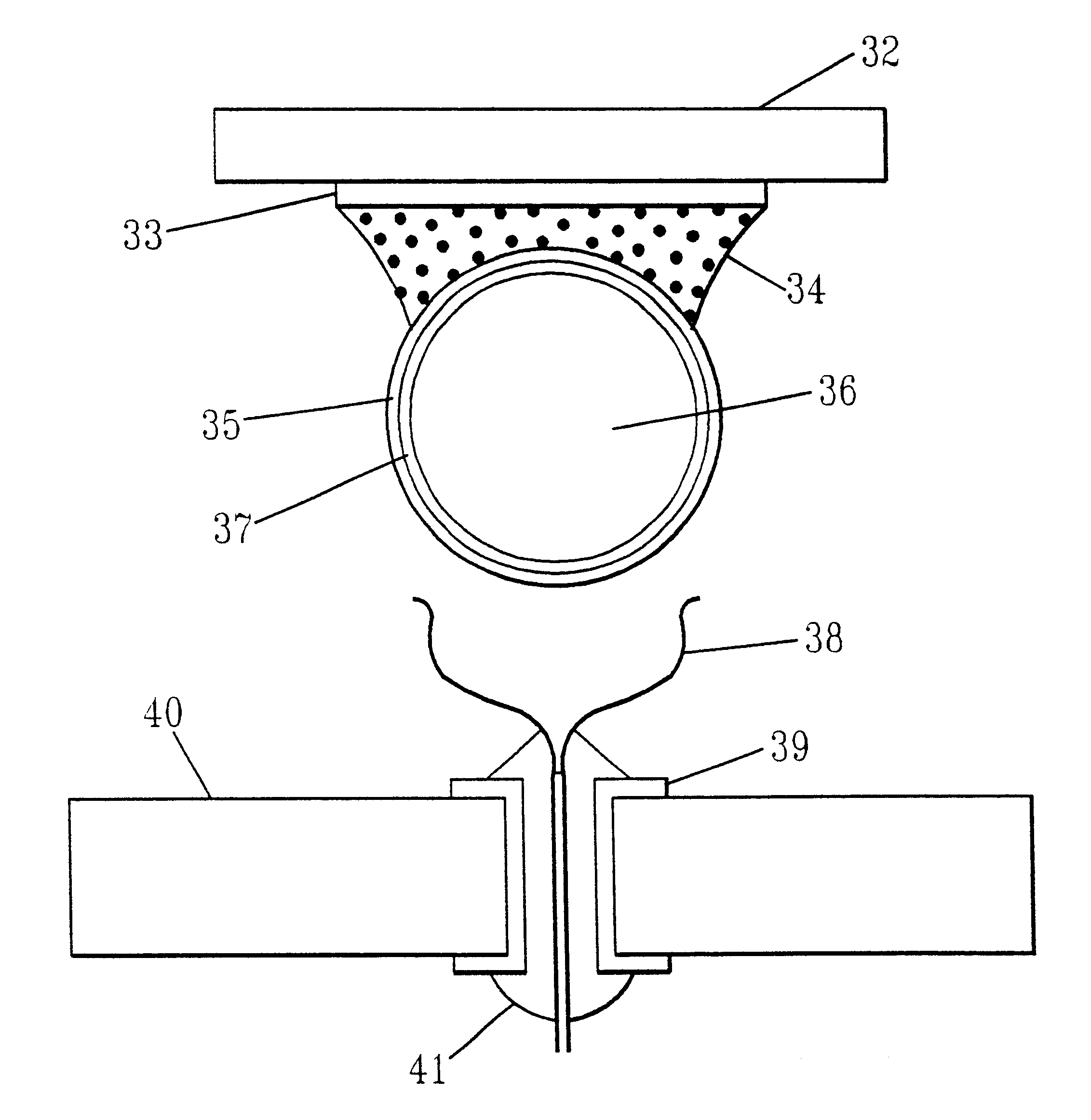
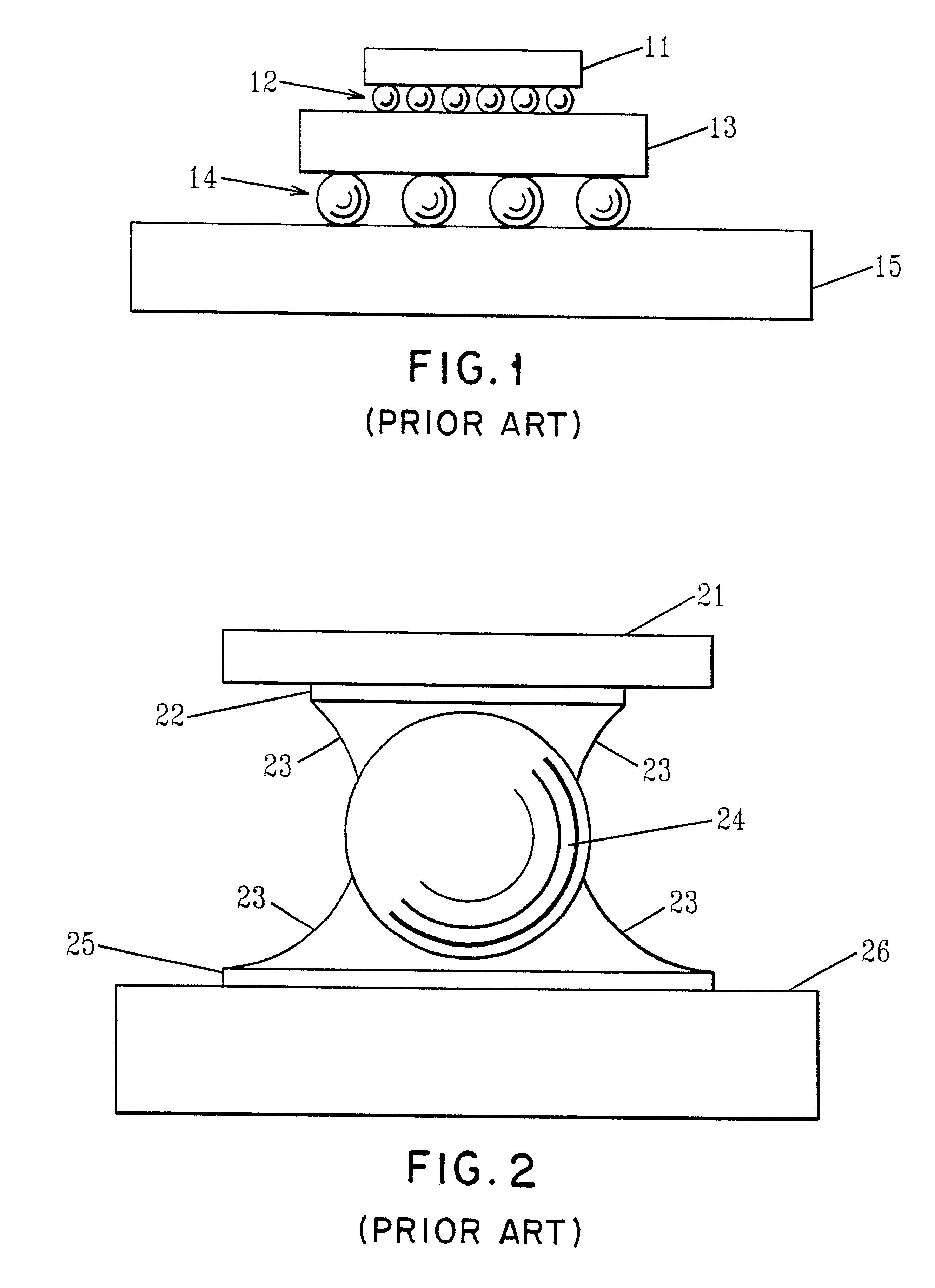
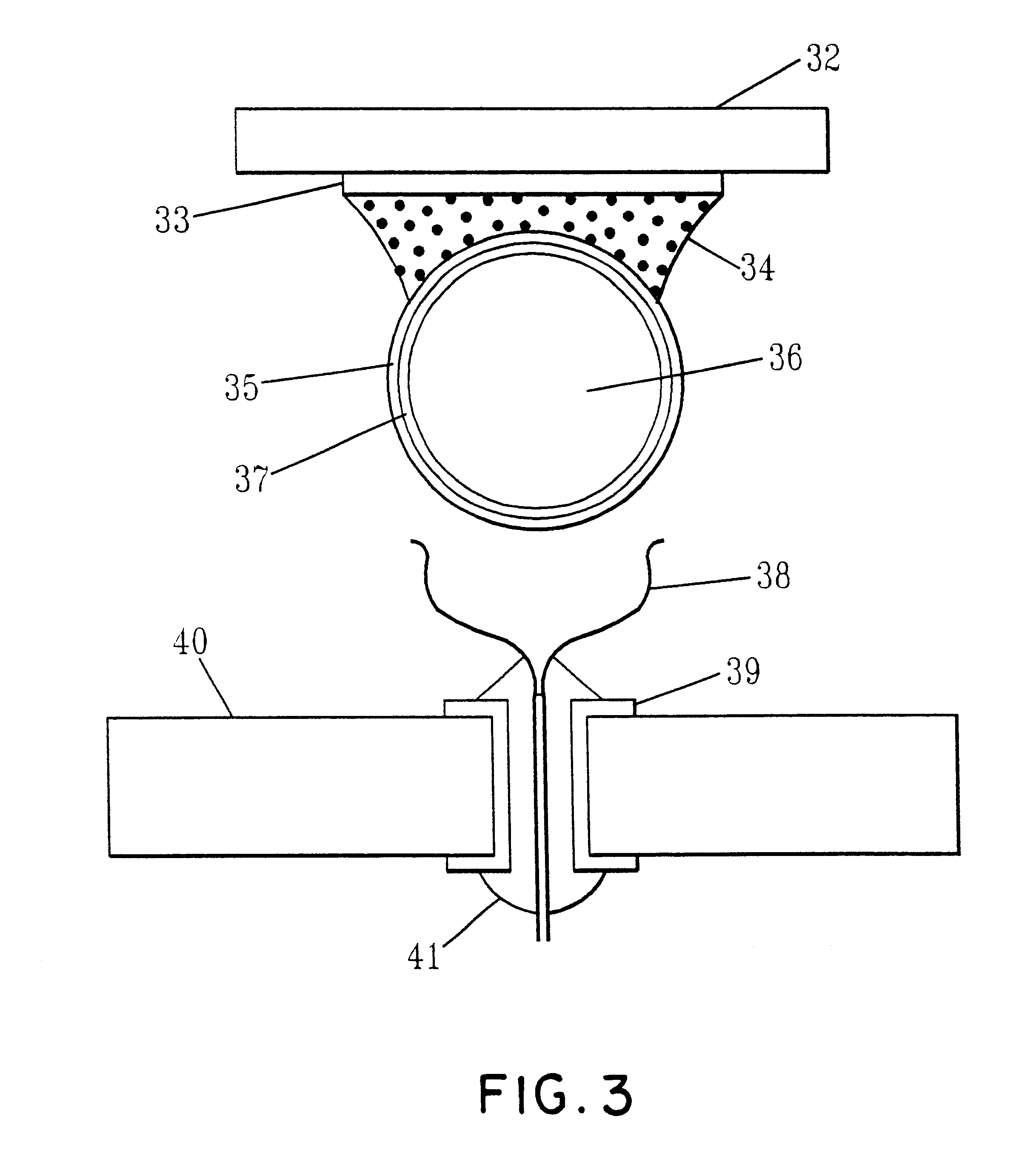
In order to facilitate an understanding of the present invention, reference will be made to FIG. 3.

In a preferred embodiment of the present invention, schematically shown in FIG. 3, the electrically conducting adhesive (ECA) is prepared by mixing a conducting powder filler, for example copper coated with a fusible material such as tin, with a thermoplastic polymer resin, such as polyimide siloxane, and a small amount of no-clean flux as taught in our previous patent application U.S. Ser. No. 08 / 641,406, disclosure of which is incorporated herein by reference. The mixture is homogenized using a three roll shear mill to ensure uniform dispersion of the powder in the polymer.

Examples of suitable electrically conductive adhesives 34 are disclosed in U.S. Ser. No. 08 / 641,406; U.S. Ser. No. 08 / 883,188; U.S. Ser. No. 60 / 052,172; U.S. Ser. No. 08 / 868,771 and U.S. Ser. No. 08 / 877,991, all of which are assigned to International Business Machines Corporation, the assignee of the present applic...


PUM

PropertyMeasurementUnit
thicknessaaaaaaaaaa
diameteraaaaaaaaaa
thicknessaaaaaaaaaa

Abstract

A socketable ball grid array structure is disclosed which comprises mechanically rigid (compared to solder alloys) balls coated with noble contact metals joined to the chip carrier terminals by means of a novel electrically conducting adhesive. Because of the nature of the filler that includes conducting particles with a fusible coating and the appropriate selection of the polymer resin used in the adhesive, the balls are attached to the module in a compliant and resilient manner while leaving the majority of the bottom surface of the balls pristine. The array of balls can therefore be plugged into mating sockets in a printed circuit board forming a demountable contact. This facilitates easy removal of the socketable BGA from a board for repair or upgrade purposes as well as allows ease of plugging and unplugging of these BGA's into test and burn-in boards.

Description

The present invention relates generally to techniques for connecting an electronic device to external circuitry, and more particularly to socketable ball grid array interconnections between microelectronic packages and printed circuit boards. In particular, it relates to ball grid arrays that can be readily demounted from the printed wiring board they are assembled on to.BACKGROUND OF INVENTIONRapid advances in microelectronic devices are continuously demanding finer pitch connections between electronic chip carriers and printed circuit boards (on the order of a few hundred micrometer pitch or less). This demand as well as the demand for low cost electronic packages have led to the increased use of surface mount technology (SMT) over the conventional plated-through-hole (PTH) technology in the recent years. At present, more than two thirds of integrated circuits (IC) including both memory and logic devices are assembled by SMT. SMT packages commonly found in a PCB assembly are leade...

Claims


Application Information

Patent Timeline
Patent Type & Authority Patents(United States)
IPC IPC(8): H01L23/498H01L23/48H05K3/34H05K3/40H05K3/32
CPCH01L23/49816H05K3/3436H05K3/4015Y10T428/12528H05K3/3447H05K2201/10234H05K2201/10333H05K2201/10962Y10S428/901H01L2924/0002H05K3/321Y10T428/256Y10T428/24917H01L2924/00Y02P70/50
Inventor CALL, ANSON J.DELAURENTIS, STEPHEN ANTHONYFAROOQ, SHAJIKANG, SUNG KWONPURUSHOTHAMAN, SAMPATHSTALTER, KATHLEEN ANN
Owner IBM CORP
Why Eureka
Try Eureka