Photomask and Method of Fabricating the Same

Inactive Publication Date: 2009-10-08
SK HYNIX INC
View PDF3 Cites 4 Cited by
  • Summary
  • Abstract
  • Description
  • Claims
  • Application Information

AI Technical Summary

Benefits of technology

[0017]According to the invention, even though poor patterns having sizes larger than a normal size are generated in a process of fabricating the photomask, the light transmittance of the portion having

Problems solved by technology

However, as the degree of integration of semiconductor devices increases, the sizes of pattern of photomasks are also gradually becoming miniaturized.
Due to this tendency, various problems may be generated in the procedure of forming fine patterns of a photomask pattern.
One of the typical problems is a pattern critical dimension (CD) error by which the pattern size of the photoma

Method used


Image

  • Photomask and Method of Fabricating the Same
  • Photomask and Method of Fabricating the Same
  • Photomask and Method of Fabricating the Same

Examples


Example

[0022]Hereinafter, a photomask and a method of fabricating the photomask in accordance with the invention will be described in detail with reference to the accompanying drawings.

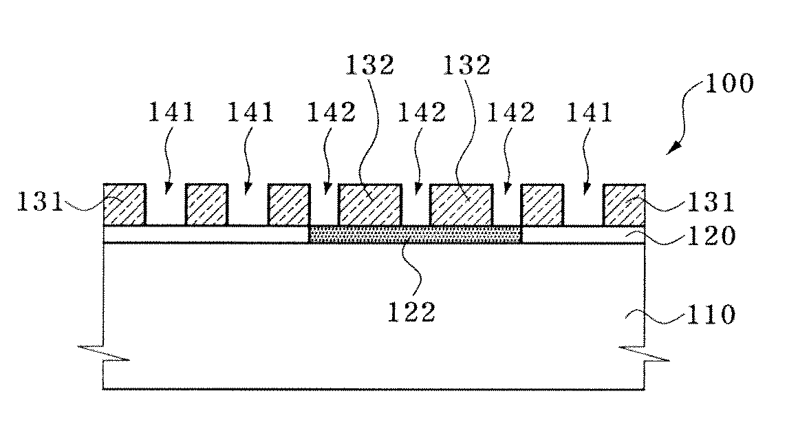
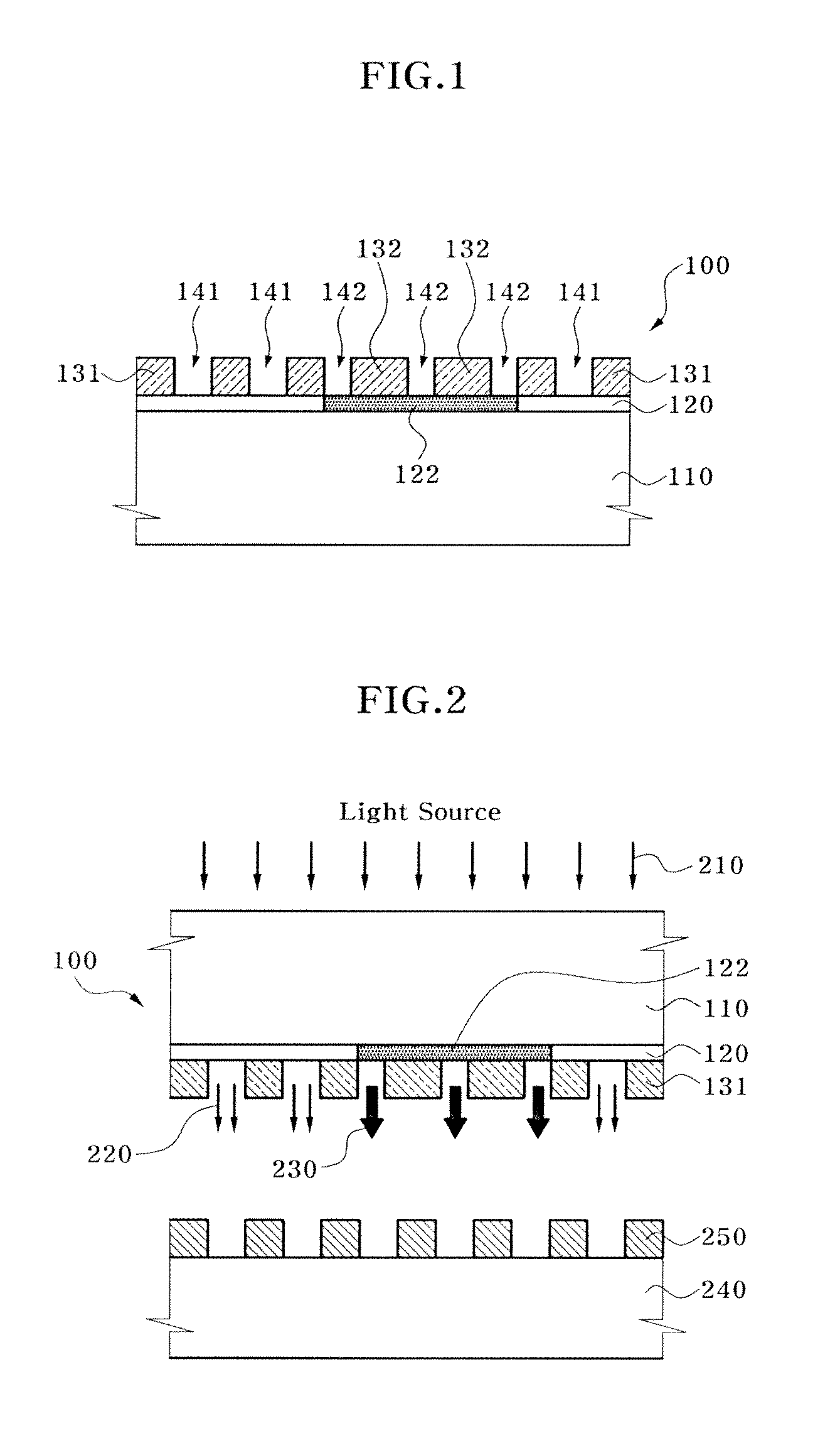
[0023]FIG. 1 is a cross-sectional view illustrating a photomask according to an embodiment of the invention. Referring to FIG. 1, in a photomask according to the present embodiment, a light transmittance control layer 120 is disposed over a light transmitting substrate 110, such as quartz, for example. Over the light transmittance control layer 120, light blocking layer patterns 131, 132 are disposed. The light transmittance control layer 120 is formed of a material having a light transmittance which varies as a function of the oxidation level of the material, and an oxidized region 122 of the control layer 120 has been oxidized. The light transmittance in the oxidized region 122 is relatively higher than the light transmittance in other regions. Though a binary photomask having the light blocking layer patt...


PUM


Abstract

A photomask comprises: a light transmitting substrate; patterns disposed over the light transmitting substrate to define a light transmitting region; and a light transmittance control layer disposed between the light transmitting substrate and the patterns having a relatively high light transmittance in a first control layer region overlapping a first portion of the light transmitting region adjacent to a poor pattern having a size larger than a normal size than in a second control layer region overlapping a second portion of the light transmitting region between normal patterns having a normal size.

Description

CROSS-REFERENCE TO RELATED APPLICATION[0001]Priority to Korean patent application number 10-2008-0032288, filed on Apr. 7, 2008, the entire disclosure of which is incorporated herein by reference, is claimed.BACKGROUND OF THE INVENTION[0002]The invention relates to a photomask used in an exposure process for fabricating a semiconductor device and a method of fabricating the same.[0003]In general, a semiconductor device is realized through various patterns on a wafer, and these patterns are formed using a photolithography process. According to a conventional photolithography process, a photoresist layer is formed on a layer to be patterned on a wafer and a predetermined portion is exposed using a photomask. Next, a photoresist layer pattern that exposes some of a surface of the layer to be patterned is formed by removing a portion of the photoresist layer, the solubility of which is changed or unchanged by the exposure, in a development process using a developing solution. Then, a pa...

Claims


Application Information

Patent Timeline
IPC IPC(8): G03F1/00
CPCG03F1/72G03F1/38
Inventor HA, TAE JOONG
Owner SK HYNIX INC
Why Eureka
Try Eureka