Apparatus and method for outputting data in semiconductor integrated circuit

Inactive Publication Date: 2009-10-15
SK HYNIX INC
View PDF8 Cites 2 Cited by
  • Summary
  • Abstract
  • Description
  • Claims
  • Application Information

AI Technical Summary

Benefits of technology

[0011]An apparatus and a method to output data in a semiconductor IC capable of minimizing a time difference between a data signal and a data strobe signal is described herein.

Problems solved by technology

If the mismatch between the data signal ‘DQ’ and the data strobe signal ‘DQS’ increases, i.e., as the time difference between the data signal ‘DQ’ and the data strobe signal ‘DQS’ deviates the predefined specification ‘tLZ’, an external system may not precisely recognize the data output from the semiconductor IC, thereby creating problems.

Method used


Image

  • Apparatus and method for outputting data in semiconductor integrated circuit
  • Apparatus and method for outputting data in semiconductor integrated circuit
  • Apparatus and method for outputting data in semiconductor integrated circuit

Examples


Embodiment Construction

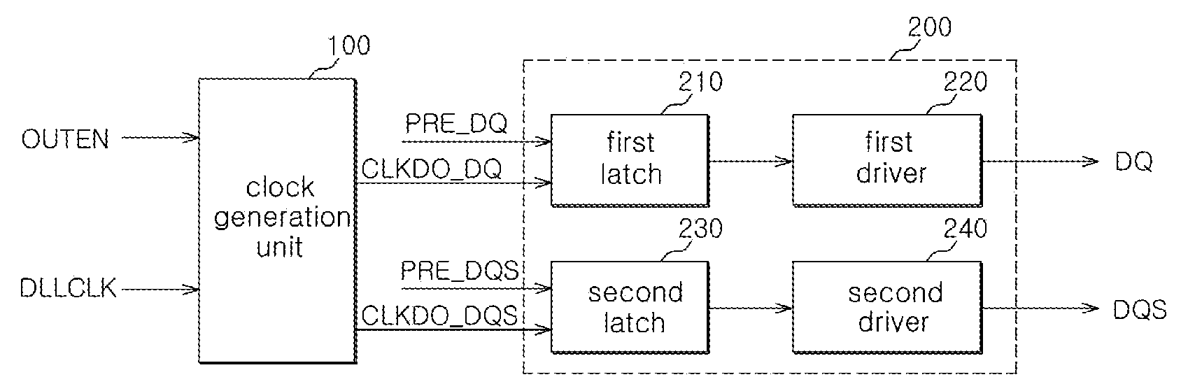
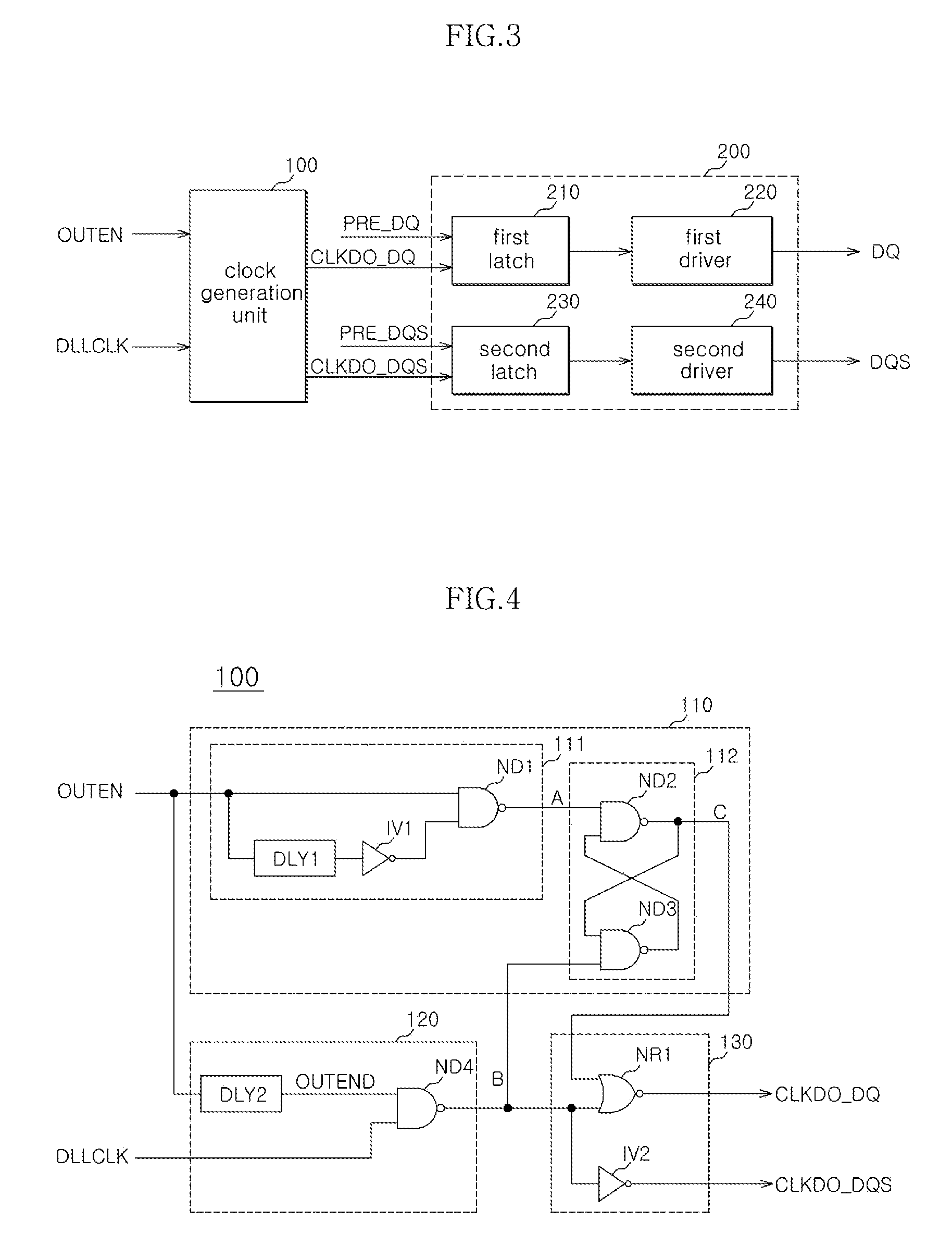
[0022]FIG. 3 is a schematic block diagram of an exemplary data output apparatus 50 of a semiconductor IC according to one embodiment. In FIG. 3, the data output apparatus 50 of a semiconductor IC can be configured to include a clock generation block 100 and a data output block 200.

[0023]The clock generation block 100 can be configured to generate a first clock signal, i.e., a data clock signal ‘CLKDO_DQ’ and a second clock signal, i.e., a data strobe clock signal ‘CLKDO_DQS’using an output enable signal ‘OUTEN’ and a delay locked loop clock signal ‘DLLCLK’, such that a data signal ‘DQ’ and a data strobe signal ‘DQS’ can have substantially the same transition timing.

[0024]The data output block 200 can include first and second latches 210 and 230, and first and second drivers 220 and 240. Accordingly, the data output block 200 can latch and drive a pre-data signal ‘PRE_DQ’in response to the data clock signal ‘CLKDO_DQ ’, and can output the data signal ‘DQ’. In addition, the data outpu...


PUM


Abstract

An apparatus for outputting data in a semiconductor integrated circuit includes a clock generation block configured to activate a first clock signal for outputting a data signal and a second clock signal for outputting a data strobe signal based on a predetermined timing, and a data output block configured to latch a pre-data signal and a pre-data strobe signal in response to the first clock signal and the second clock signal, respectively.

Description

CROSS-REFERENCES TO RELATED APPLICATION[0001]The present application claims priority under 35 U.S.C. § 119(a) to Korean application number 10-2008-0033315, filed on Apr. 10, 2008, in the Korean Intellectual Property Office, which is incorporated herein by reference in its entirety as if set forth in full.BACKGROUND[0002]1. Technical Field[0003]The embodiments described herein relate to a semiconductor integrated circuit (IC), and more particularly, to a apparatus and a method for outputting data in a semiconductor IC.[0004]2. Related Art[0005]In general, a semiconductor IC includes an apparatus to output a data signal ‘DQ’ and a data strobe signal ‘DQS’ indicative of timing for reading the data signal ‘DQ’ from an exterior of the semiconductor IC in response to a read command.[0006]FIG. 1 is a schematic block diagram of a conventional data output apparatus of a semiconductor IC. In FIG. 1, the data output apparatus 10 includes latches 1 and 2 and drivers 3 and 4. A pre-data signal ‘...

Claims


Application Information

Patent Timeline
IPC IPC(8): G11C7/00G11C8/18
CPCG06F1/06G11C7/1051H03K5/135G11C7/1066G11C7/106G11C7/10G11C7/22
Inventor JEON, BYUNG DEUK
Owner SK HYNIX INC
Why Eureka
Try Eureka