Thermoelectric module and a method of manufacturing the same

a technology of thermoelectric modules and manufacturing methods, applied in the manufacture/treatment of thermoelectric devices, thermoelectric device junction materials, electrical apparatuses, etc., can solve the problems of short circuit, inability to reduce the arbitrary shape of p-type and n-type thermoelectric elements, and the possibility of becoming a barrier for narrow pitch and high density mounting and module miniaturization

Inactive Publication Date: 2005-06-30
FURUKAWA ELECTRIC CO LTD
View PDF3 Cites 82 Cited by
  • Summary
  • Abstract
  • Description
  • Claims
  • Application Information

AI Technical Summary

Benefits of technology

[0172] The embodiment 4-7 according to the invention is a method for a narrow pitch bonding of the micro element comprising the step of determining the amount of the bonding material so that the excess part of the bonding material does not occur to swell out from the circumference of the micro elements and the electric circuit...

Problems solved by technology

The problem with the conventional method is a method using a dicing saw when making a P-type thermoelectric element and a N-type thermoelectric element.
This is a disadvantage as unable to reduce an arbitrary shape of a P-type and N-type thermoelectric element.
As the size of the electronic element or the semiconductor element become further miniaturized and, in that a micro electric element and a micro semiconductor element, the bonding material inserted between the electric circuit metal layer on the substrate and the electrodes of a micro electronic element or a micro semiconductor product is likely to swell out around the circumference of the electrodes and that may cause a short circuit problem.
Therefore, if miniaturization (i.e., downsizing) of an electronic element or a semiconductor element progresses further, it is likely to become a barrier for a narrow pitch and high density mounting and module miniaturization.
Consequently, the micro element gets wet with the bonding material such as a soldering material and new chemical compound is made and that degrades its performance.
In that, if the thickness of bonding material layer is thicker than the pre-designed value in order to fill a gap, it is likely to cause a short circuit.
Consequently, there has been a problem that the micro element gets wet with the bonding material such as a soldering material and new chemical compound is made and hence that degrades its performance.
Also, there has been a problem with the bulging bonding material restricting a progress of narrow pitch and high density mounting and module miniaturization.
Furthermore, if the t...

Method used


Image

  • Thermoelectric module and a method of manufacturing the same
  • Thermoelectric module and a method of manufacturing the same
  • Thermoelectric module and a method of manufacturing the same

Examples


Embodiment Construction

[0297] Referring to the drawings, the embodiments of the invention will be described below, however the present invention is not limited to those embodiments described below but also includes any embodiments which a person skilled in the art may come to think by combination of the embodiments described here.

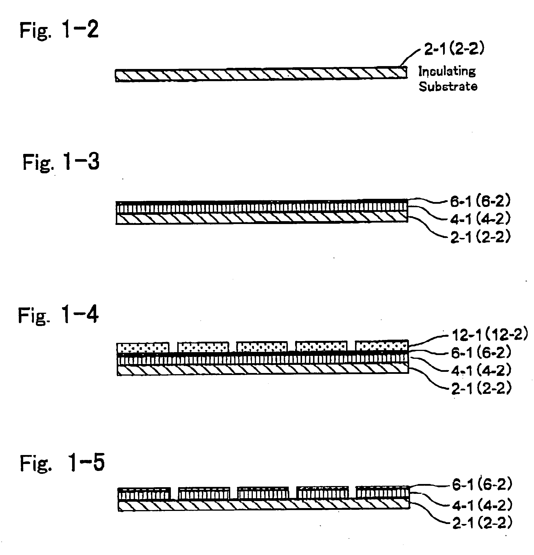
[0298] Hereinafter, referring to FIG. 1-1 through FIG. 1-15, the embodiments of the invention will be described.

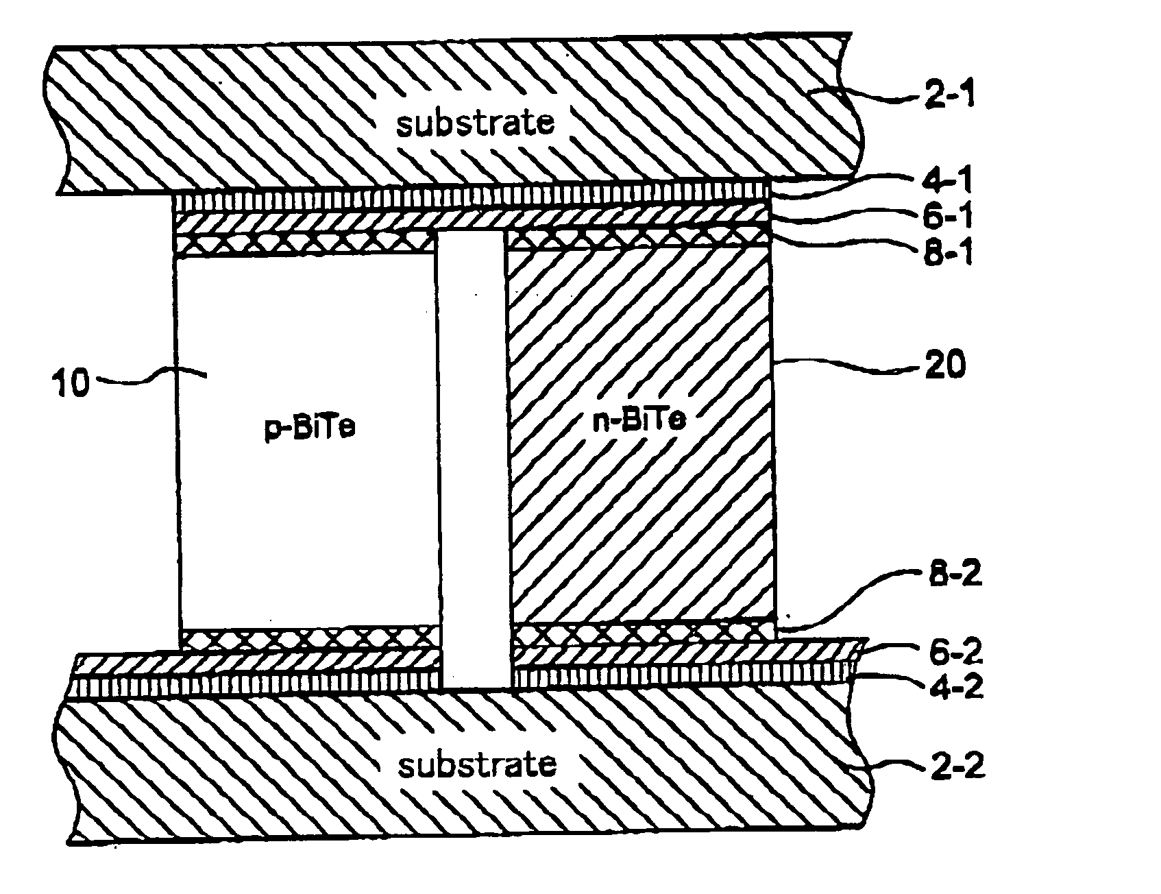
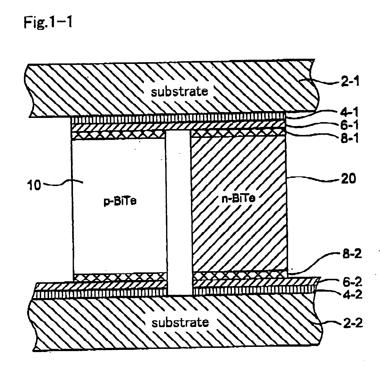
[0299]FIG. 1-1 shows a schematic cross sectional view of the thermoelectric element in accordance with the invention. The P-type semiconductor 10 and the N-type semiconductor 20 are placed between the top side substrate 2-1 and the bottom side substrate 2-2 and connected to the electric circuit metal layer 4-1 via a blast stopper layer 6-1 which will be detailed later, and the P-type semiconductor 10 in the left side in the drawing is connected to the N-type semiconductor 20 in the right side, similarly the N-type semiconductor in the right side is connected further t...


PUM


Abstract

A thermoelectric module comprises an upper insulating substrate and a lower insulating substrate; an upper electric circuit metal layer and a lower electric circuit metal layer bonded respectively to the surfaces of said insulating substrates which are positioned face to face; an upper blast stopper layer and a lower blast stopper layer fabricated respectively on said electric circuit metal layers; an upper bonding layer and a lower bonding layer fabricated respectively on said blast stopper layers; and a plurality of -shaped elements consisting of a pair of the P-type semiconductor element and N-type semiconductor element which are fabricated between said upper and lower bonding layers and are electrically connected in series through said upper and lower blast stopper layers.

Description

CROSS-REFERENCE TO RELATED APPLICATION [0001] The present application is a continuation of PCT / JP03 / 07194, filed on Jun. 6, 2003, the entire contents of which are incorporated herein by reference, and which claims the benefit of the dates of the earlier filed Japanese Patent Applications, having JP 2002-165094 filed on Jun. 6, 2002, JP 2002-292570 filed on Oct. 4, 2002, JP 2002-297465 filed on Oct. 10, 2002, JP 2003-076217 filed on Mar. 19, 2003, JP 2003-078117 filed on Mar. 20, 2003 and JP 2003-153770 filed on May 30, 2003.TECHNICAL FIELD [0002] This invention relates to a thermoelectric module which comprises a P-type and a N-type semiconductor, more particularly a thermoelectric module having a function of a power generator by temperature difference, namely Seebeck effect, or a function of an electric cooler and heater, namely Peltier effect, and a method for manufacturing. Furthermore, this invention relates to a module including a micro element such as a micro electronic elemen...

Claims


Application Information

Patent Timeline
IPC IPC(8): H01L35/16H01L35/28H01L35/32H01L35/34
CPCH01L35/34H01L35/32H10N10/01H10N10/17
Inventor UEKI, TATSUHIKONAKAMURA, YOSHINORIHIRATANI, YUJI
Owner FURUKAWA ELECTRIC CO LTD
Why Eureka
Try Eureka