Electrical connectors and circuit boards having non-ohmic plates

a technology of electrical connectors and circuit boards, applied in the direction of high-frequency circuit adaptations, electrical apparatus construction details, coupling device connections, etc., can solve the problems of connectors not being able to effectively use non-ohmic trace, affecting the performance of electrical connectors, and -ohmic trace affording limited effect on electrical performan

Active Publication Date: 2009-10-29
COMMSCOPE TECH LLC
View PDF10 Cites 44 Cited by
  • Summary
  • Abstract
  • Description
  • Claims
  • Application Information

AI Technical Summary

Benefits of technology

[0005]In one embodiment, an electrical connector includes a housing and a plurality of contacts within the housing that are configured to engage with mating contacts of a mating connector. The contacts form at least a first differential pair and a second differential pair. The electrical connector also includes a circuit board housed within the housing. The circuit board has a substrate body formed from a dielectric material and includes a first trace electrically coupled to a contact of the first differential pair and a second trace electrically coupled to a contact of the second differential pair. At least one of the first and second traces is an open-ended trace. The circuit board also has a non-ohmic plate that is positioned adjacent to the traces. The plate is positioned to electromagnetically couple the first and second traces to each other and the non-ohmic plate and traces are configured for a desired electrical performance.

Problems solved by technology

The electrical connectors have traditionally been used for data transmission, wherein the performance of the electrical connectors may be negatively affected by, for example, near-end crosstalk (NeXT) and / or return loss.
However, the known electrical connector has not been able to effectively use the non-ohmic trace to improve performance and, in fact, the non-ohmic traces have afforded a limited effect on the electrical performance.

Method used


Image

  • Electrical connectors and circuit boards having non-ohmic plates
  • Electrical connectors and circuit boards having non-ohmic plates
  • Electrical connectors and circuit boards having non-ohmic plates

Examples


Embodiment Construction

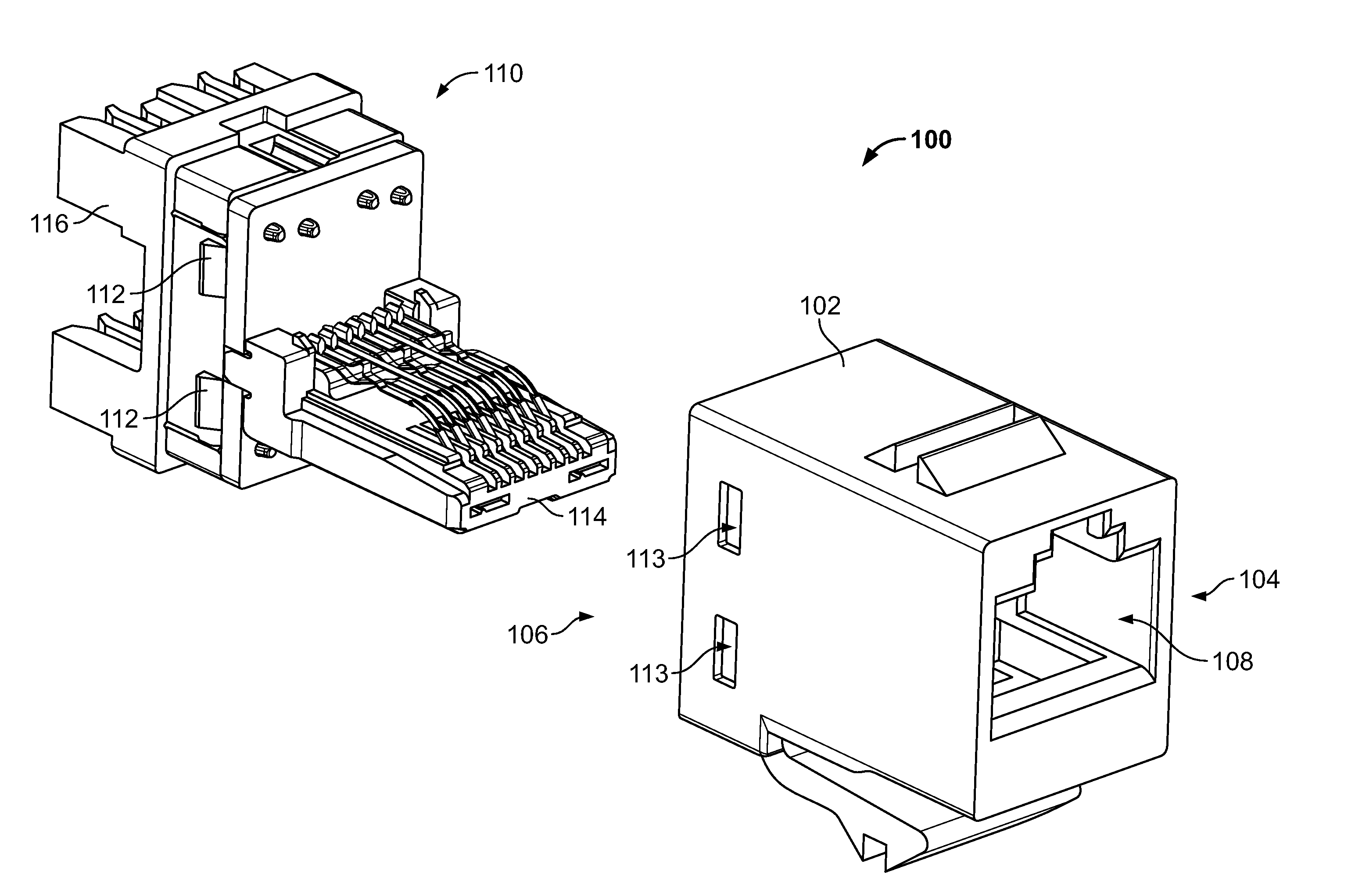
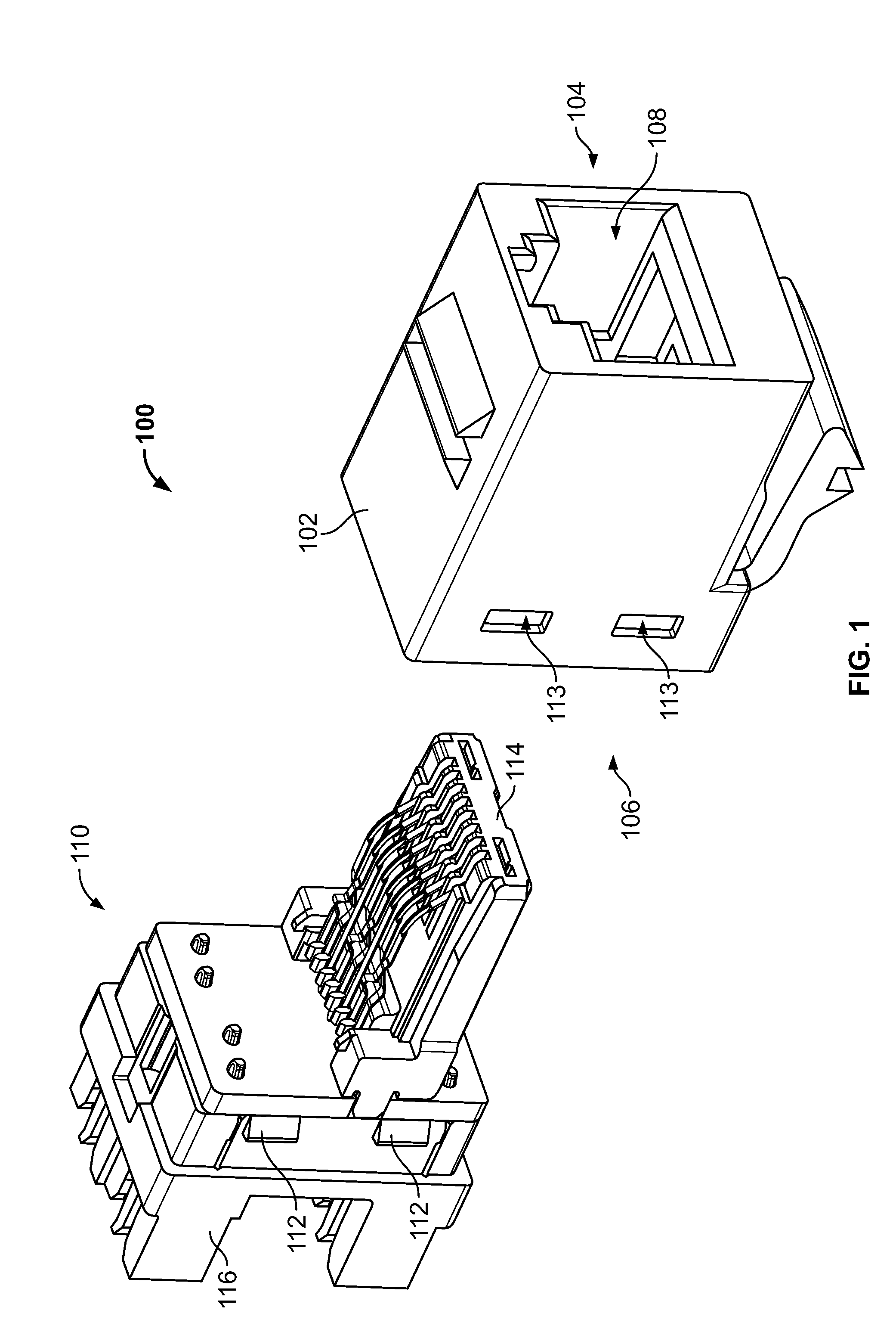
[0022]FIG. 1 is an exploded view of an electrical connector 100 formed in accordance with one embodiment. As shown, the connector 100 is a modular connector, such as an RJ-45 jack assembly. The connector 100 is configured for joining with a mating plug (not shown). While the connector 100 is shown and described with reference to an RJ-45 jack assembly the subject matter herein may be used with other types of connectors, and the RJ-45 jack assembly is merely illustrative of an exemplary embodiment. The connector 100 may be used for data and / or power transmission and may also be used with differential pair multi-conductor transmission lines.

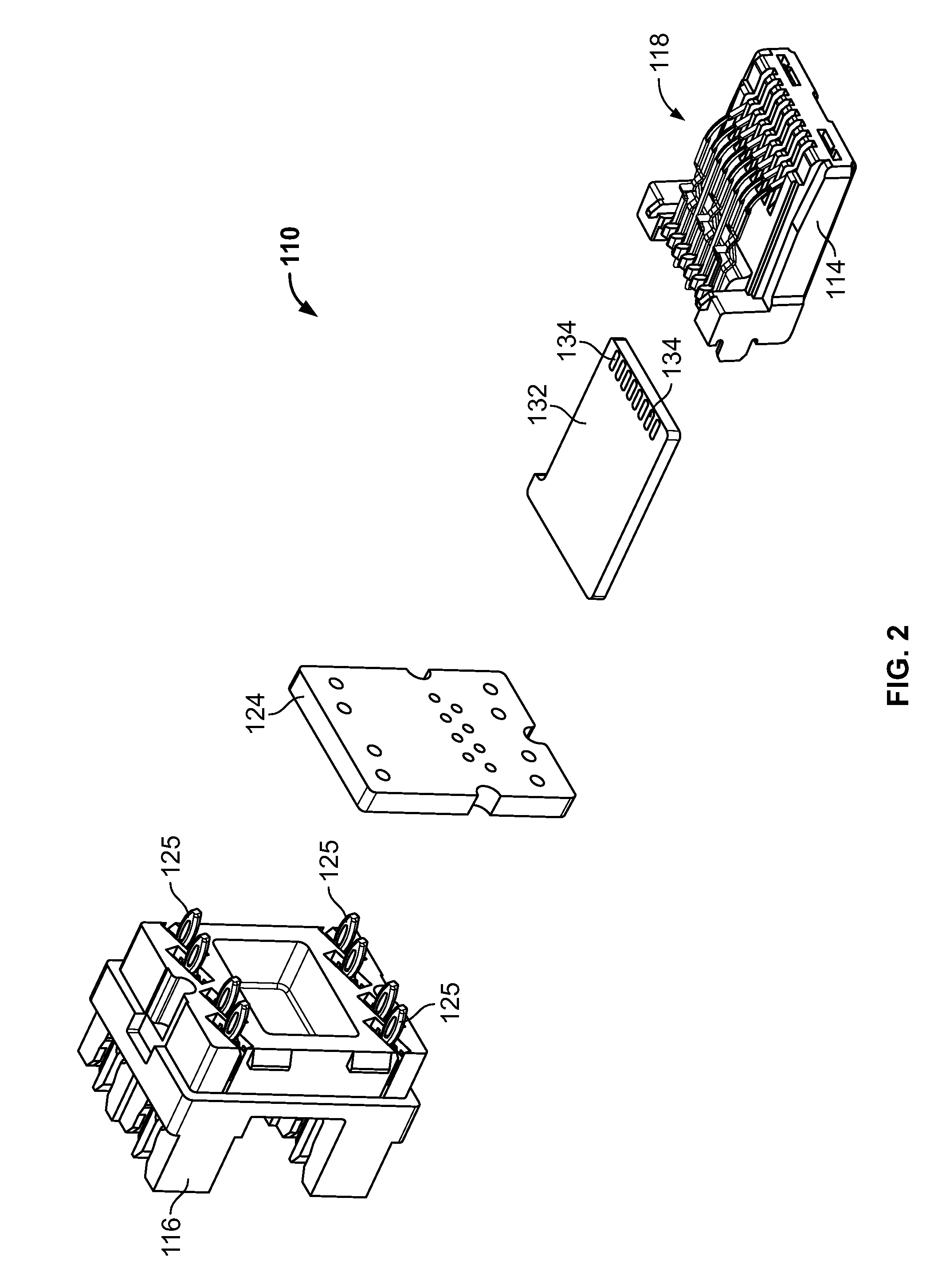
[0023]As will be discussed in greater detail below, embodiments described herein include circuit boards that utilize non-ohmic plates to improve the electrical performance of the connector 100 or any other device that the circuit board(s) may be used with. For example, the connector 100 may use one or more non-ohmic plates to reduce near-end crosst...


PUM


Abstract

An electrical connector includes a housing and a plurality of contacts within the housing that are configured to engage with mating contacts of a mating connector. The contacts form at least a first differential pair and a second differential pair. The electrical connector also includes a circuit board housed within the housing. The circuit board has a substrate body formed from a dielectric material and includes a first trace electrically coupled to a contact of the first differential pair and a second trace electrically coupled to a contact of the second differential pair. At least one of the first and second traces is an open-ended trace. The circuit board also has a non-ohmic plate that is positioned adjacent to the traces. The plate is positioned to electromagnetically couple the first and second traces to each other and the non-ohmic plate and traces are configured for a desired electrical performance.

Description

BACKGROUND OF THE INVENTION[0001]The subject matter herein relates generally to electrical connectors and more particularly to electrical connectors that have circuit boards and that utilize differential pairs.[0002]Electrical connectors are commonly used in telecommunication systems. The electrical connectors, such as modular jacks and modular plugs, may provide interfaces between successive runs of cable in such systems and between cables and electronic devices. The electrical connectors may include contacts that are arranged according to known industry standards, such as Electronics Industries Alliance / Telecommunications Industry Association (“EIA / TIA”)-568. The electrical connectors have traditionally been used for data transmission, wherein the performance of the electrical connectors may be negatively affected by, for example, near-end crosstalk (NeXT) and / or return loss.[0003]To compensate for the crosstalk and / or to improve the return loss, known techniques have focused on a...

Claims


Application Information

Patent Timeline
Patent Type & Authority Applications(United States)
IPC IPC(8): H01R13/66H01R24/00
CPCH01R13/6658H05K1/0228H05K1/0237H05K1/0239H05K1/162Y10S439/941H05K2201/09672H05K2201/10189H01R13/719H01R13/6466H01R13/6469H05K2201/09236H01R13/6464
Inventor PEPE, PAUL JOHNTOBEY, SHAWN PHILLIPMUIR, SHELDON EASTONBOPP, STEVEN RICHARD
Owner COMMSCOPE TECH LLC
Why Eureka
Try Eureka