Apparatus for current-to-voltage integration for current-to-digital converter

a current-to-digital converter and current-to-voltage technology, applied in the field of current-to-voltage integrators, can solve the problems of thermal noise, unfavorable sample reset voltage, and thermal noise present in the switch used for sampling operation or amplifier, so as to reduce the demands on the reference voltage source, the effect of reducing charge injection and kt/c errors

Inactive Publication Date: 2009-11-05
CUSTOM ONE DESIGN
View PDF3 Cites 97 Cited by
  • Summary
  • Abstract
  • Description
  • Claims
  • Application Information

AI Technical Summary

Benefits of technology

The present invention improves current-to-voltage integrators by reducing errors caused by capacitor switching and operational amplifier noise during the reset cycle. This improvement reduces the demand on the reference voltage source and is useful in analog-to-digital converters for X-ray-to-digital data acquisition systems of CT systems.

Problems solved by technology

The technical problem addressed in this patent text is the need for a more precise and accurate data acquisition system for CT imaging. The large dynamic range and accuracy required for CT systems requires very precise data acquisition systems, including the charge-to-digital converter. However, the current method of resetting the integrating capacitors to zero volts during the reset cycle preceding each integration cycle introduces thermal noise, which causes undesired voltage errors. The patent text proposes new methods and architectures for the integrators used as an input current-to-voltage converting stage of complex CT systems to reduce these errors.

Method used


Image

  • Apparatus for current-to-voltage integration for current-to-digital converter
  • Apparatus for current-to-voltage integration for current-to-digital converter
  • Apparatus for current-to-voltage integration for current-to-digital converter

Examples


Embodiment Construction

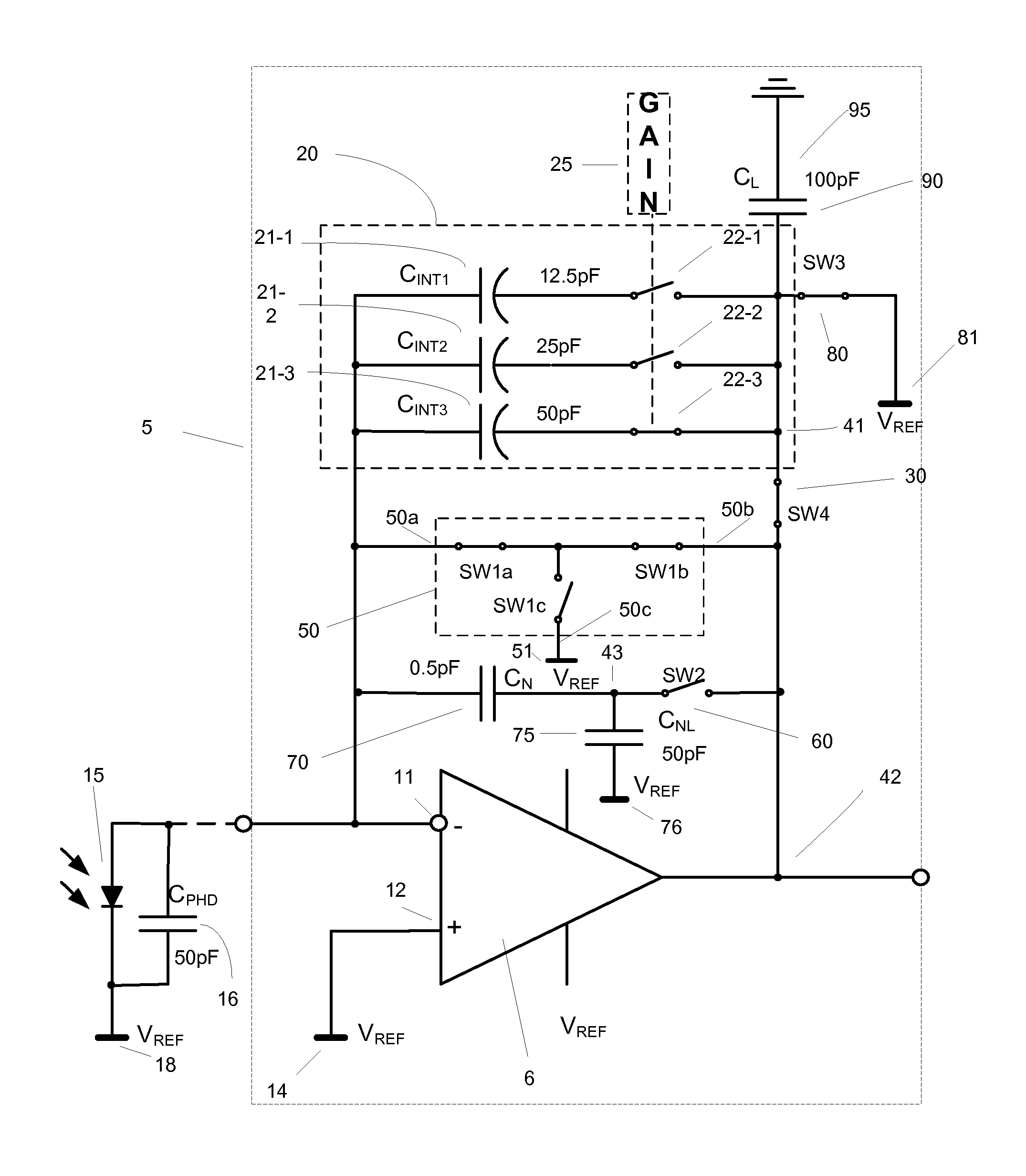
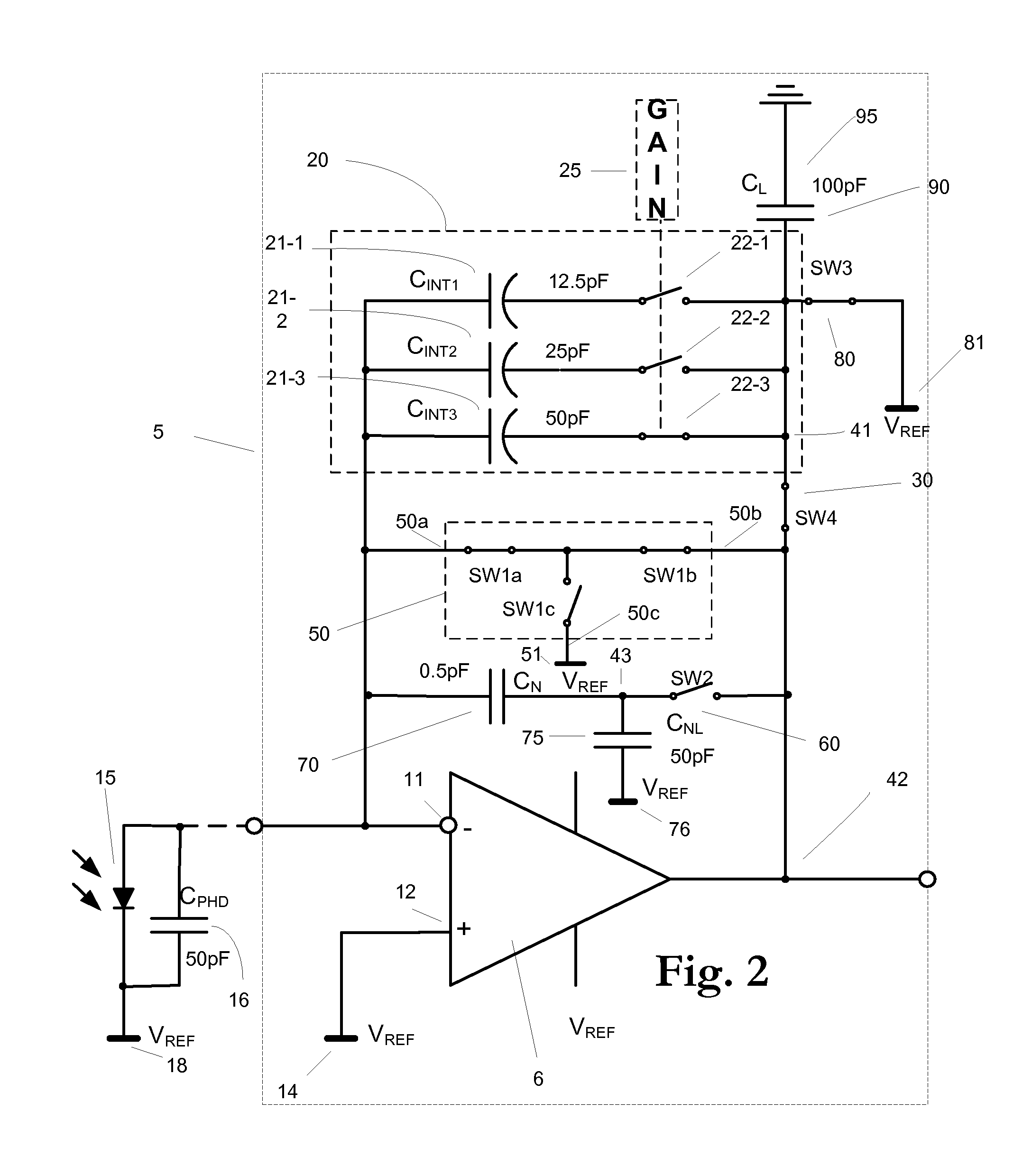
[0038]FIG. 2 depicts one embodiment of a current-to-voltage integrator 5 in accord with the present invention. FIG. 2 also shows the connection of an ideal photodiode 15 as it is supposed to be connected to the integrator 5, together with the parasitic capacitance 16 associated with this connection. The connection of an actual photodiode 15′ may differ significantly from the connection of the ideal photodiode 15 and may include additional switches, etc.

[0039]Still referring to FIG. 2, current-to-voltage integrator 5 includes an operational amplifier 6 having an inverting (−) input connected to node 11, and a non-inverting (+) input connected by node 12 to reference voltage VREF at node 14 that replaces the “virtual ground” normally used in such integrator circuits. Other embodiments may utilize another suitable bias voltage node 14′, in which case the “virtual reference voltage” referred to hereinafter would be equal to that bias voltage.

[0040]Inverting input node 11 is indirectly c...


PUM


Abstract

Methods and apparatus for improved current-to-voltage integrators reducing charge injection and kT/C errors from capacitor switching and intrinsic operational amplifier noise (i.e., offset, 1/f noise, thermal noise) during the reset cycle of the integrator, simultaneously reducing demands on the reference voltage source, using correlated double sampling to compensate for DC offset and low frequency op-amp noises, and “fake” integration and a capacitor divider to eliminate or significantly reduce kT/C noise and charge injection.

Description


Claims


Application Information

Patent Timeline
Owner CUSTOM ONE DESIGN
Why Eureka
Try Eureka