Radiation image detector
a detector and radiation image technology, applied in the direction of optical radiation measurement, material analysis using wave/particle radiation, instruments, etc., can solve the problems of poor residual image lag characteristics, reduced sensitivity, image quality deterioration, etc., to reduce the charge injection into the edges of the detecting electrode, suppress image defects, and reduce electrical fields
- Summary
- Abstract
- Description
- Claims
- Application Information
AI Technical Summary
Benefits of technology
Problems solved by technology
Method used
Image
Examples
first embodiment
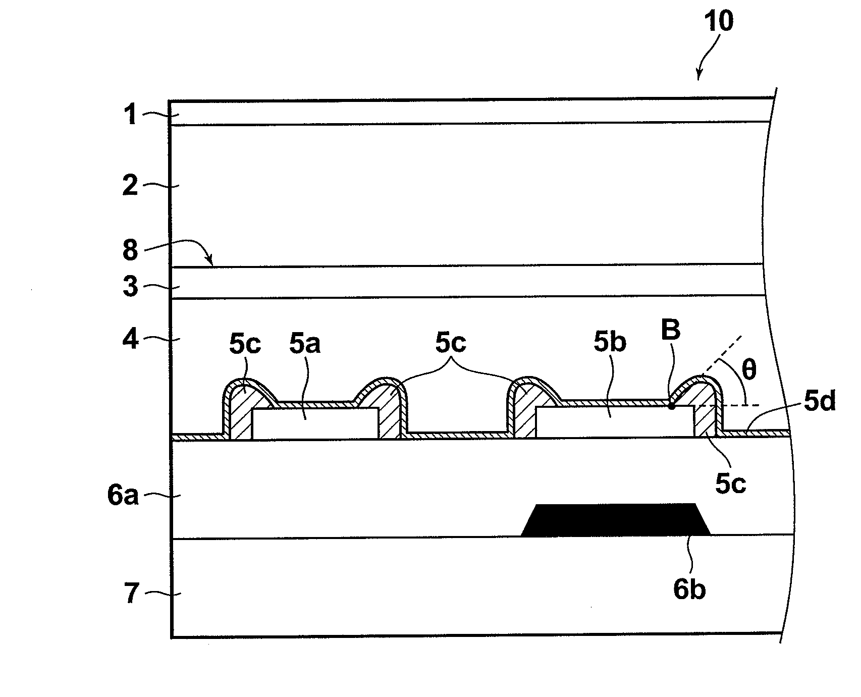
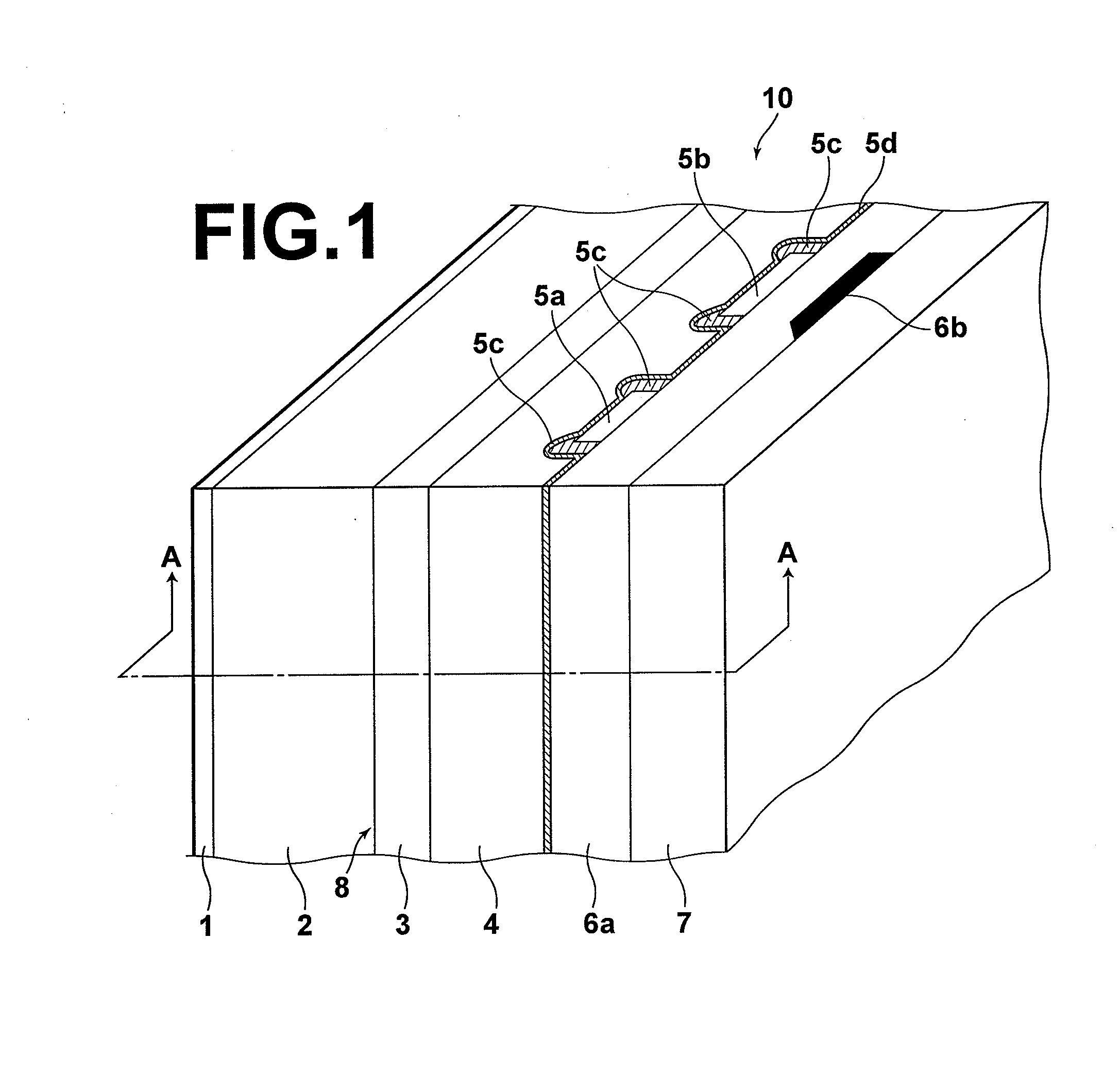
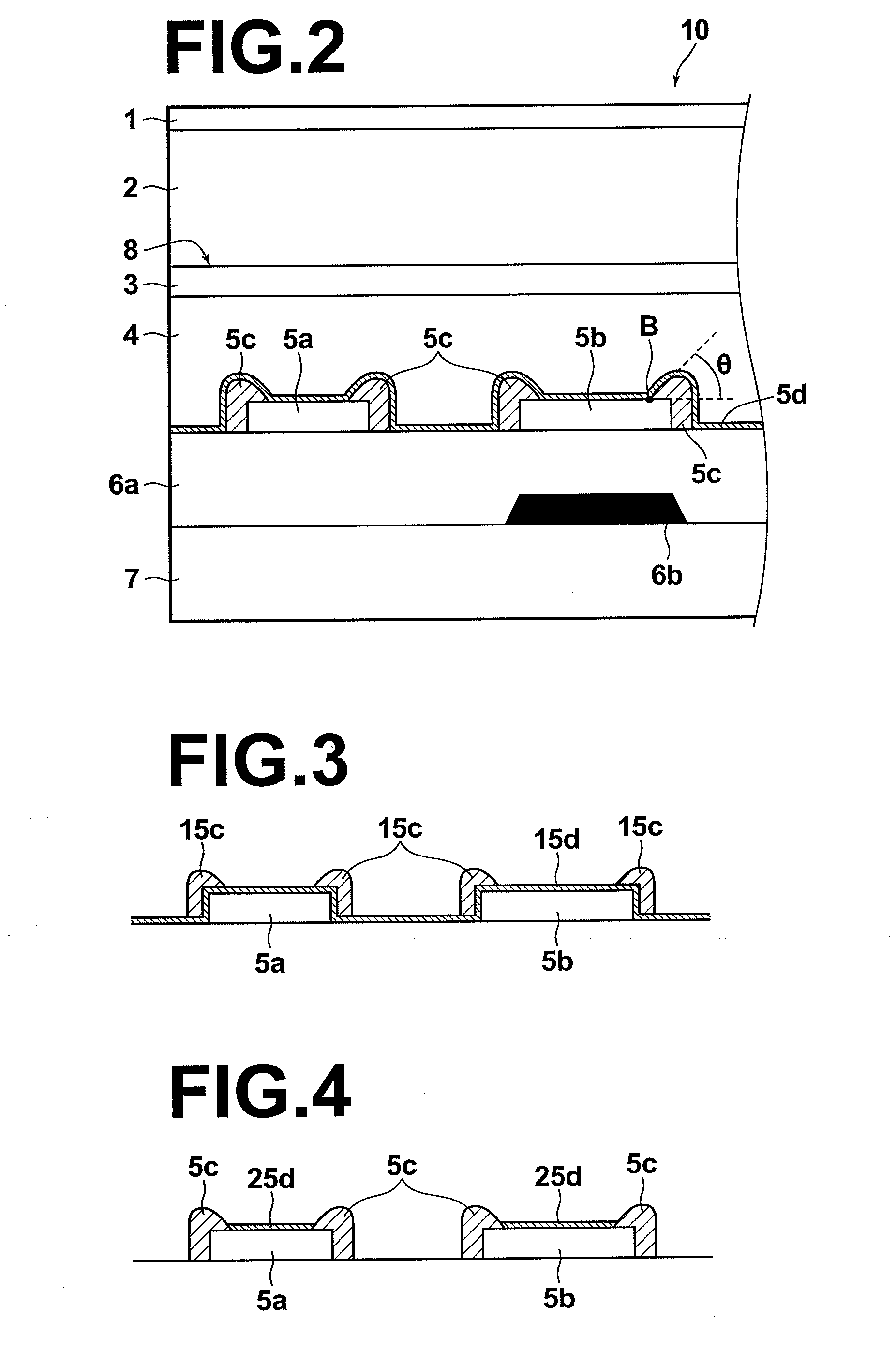
[0091]Note that in the first embodiment described above, the radiation image detector 10 comprises the charge pair generating first linear electrodes 5a and the non charge pair generating second linear electrodes 5b, both of which are provided with the dielectrics 5c and the charge injection preventing layer 5d. In the case that two types of electrodes are provided, however, improvements in image faults, sensitivity, and residual image characteristics can be obtained by only providing one of the types of electrodes with the dielectrics 5c and the charge injection preventing layer 5d.
second embodiment
[0092]Next, a radiation image detector 30 according to the present invention will be described. FIG. 6 is a schematic view that illustrates the construction of the radiation image detector 20.
[0093]The radiation image detector 30 of the second embodiment employs the electrical readout method. The radiation image detector 30 is formed by stacking: a first electrode layer 31 that transmits recording electromagnetic waves bearing radiation image information; a photoconductive layer 32 that generates charges when irradiated by the recording electromagnetic waves transmitted through the first electrode layer 31; and a plurality of pixel electrodes 35, which are detecting electrodes for detecting signals corresponding to the charges generated in the photoconductive layer 32; in this order, as illustrated in FIG. 6. Each of the pixel electrodes 35 is connected to an accumulating capacitor 36, for accumulating the electric charges collected by the pixel electrode 35, and a switching element...
PUM
 Abstract
Description
Claims
Application Information
 - R&D
- Intellectual Property
- Life Sciences
- Materials
- Tech Scout
- Unparalleled Data Quality
- Higher Quality Content
- 60% Fewer Hallucinations
Browse by: Latest US Patents, China's latest patents, Technical Efficacy Thesaurus, Application Domain, Technology Topic, Popular Technical Reports.
© 2025 PatSnap. All rights reserved.Legal|Privacy policy|Modern Slavery Act Transparency Statement|Sitemap|About US| Contact US: help@patsnap.com


