

Circuit and method for reducing charge injection and clock feed-through in switched capacitor circuits
- Summary
- Abstract
- Description
- Claims
- Application Information
AI Technical Summary
Benefits of technology
Problems solved by technology
Method used
Image

Examples
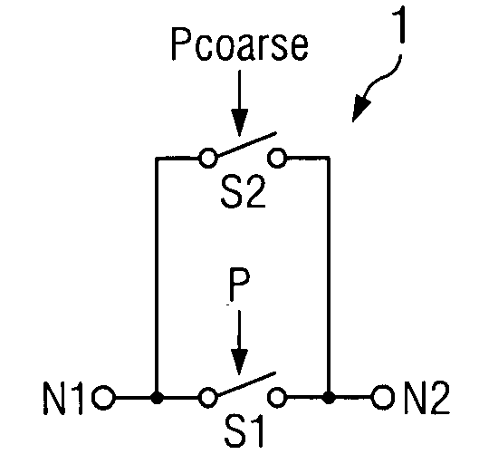
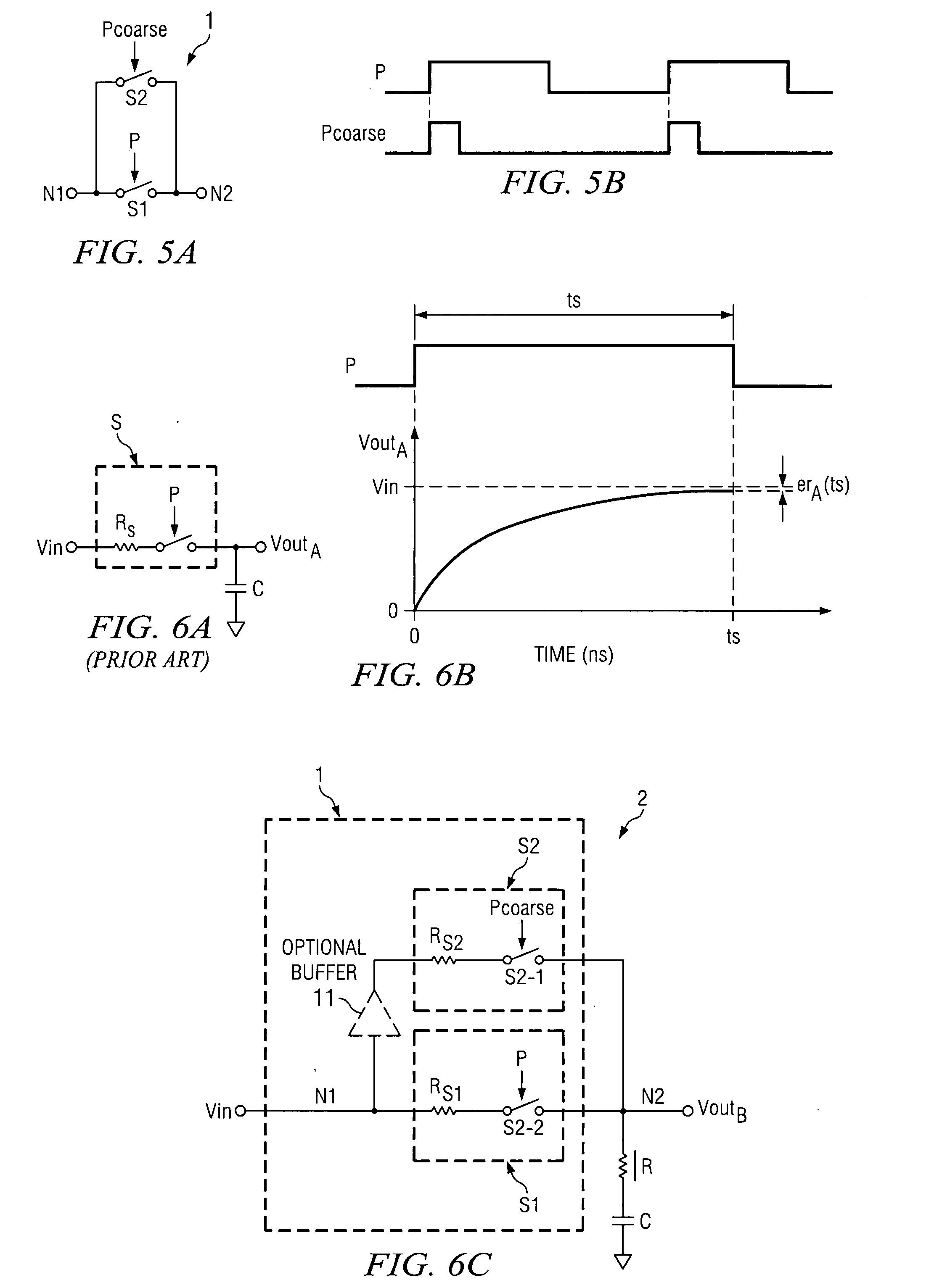
embodiment 3
[0066]FIG. 7C shows an embodiment 3 of the invention applied to transistor switch S2 of FIG. 7A to improve both linearity and common-mode rejection of that circuit. As indicated in FIG. 7C, switch S2 is controlled by P1 and switches S1p and S1n are controlled by P1d. In the circuit of FIG. 7C, MOS transistor switch S2coarse, which is controlled by clock signal P1coarse of FIG. 7D, is provided in parallel with MOS transistor switch S2, and the size (i.e., channel width W) of switch S2 is reduced. The size reduction of switch S2 results in proportional reduction of charge injection and clock feed-through and correspondingly results in improved linearity and common-mode rejection of the switched-capacitor circuit 3.
embodiment 4
[0067]FIG. 7E shows an embodiment 4 of the invention applied not only to switch S2 of in FIG. 7A, but also to switches S1p and S1n to further improve both linearity and common-mode rejection of the circuit shown in FIG. 7A. In the switched-capacitor circuit 4 of FIG. 7E the additional switches S1pcoarse and S1ncoarse both controlled by clock signal P1coarse, are provided in parallel with switches S1p and S1n, respectively, and the size W of switches S1p and S1n is reduced. The size reduction of switches S1p and S1n results in proportional reduction of channel charge injection and clock feed-through from those switches and results in further improvement of linearity and common-mode rejection of the switched-capacitor circuit 4.
[0068]FIG. 8A shows another prior art configuration of the differential input-sampling portion of a switched capacitor circuit commonly used, for example, in delta-sigma analog-to-digital converters. FIG. 8B shows the clock signals P1 and P1d. This circuit is s...
PUM
 Abstract
Description
Claims
Application Information