Method and apparatus providing analog row noise correction and hot pixel filtering

a technology of applied in the field of analog row noise correction and hot pixel filtering, can solve the problems of vertical shading, distortion of the resulting digital image, and increased physical non-uniformity of the array

Active Publication Date: 2009-11-05
APTINA IMAGING CORP
View PDF23 Cites 28 Cited by
  • Summary
  • Abstract
  • Description
  • Claims
  • Application Information

AI Technical Summary

Problems solved by technology

However, various noise sources can affect individual pixel outputs and thus distort the resulting digital image.
As CMOS pixel arrays increase in size to obtain higher resolution, the physical non-uniformity of the arrays becomes more prominent.
One issue is the signal variation between rows that can result in vertical shading.
The above solution to row noise may be adversely affected by what is known as “hot” pixels.
Hot pixels are typically caused by process defects such as e.g., silicon defects, metallic contamination, stress, etc.
That is, the values of the hot reference pixels adversely affect the row noise compensation average discussed above: this improper average will cause an incorrect compensation offset to be applied to the image pixels in that row, causing the entire row of image pixels to have inaccurate values.
Noise correction and or hot pixel filtering in the digital domain suffers from a lack of accuracy because other noise is introduced between the analog pixel and the digital processing circuits that make row noise correction and / or hot pixel filtering less accurate.

Method used


Image

  • Method and apparatus providing analog row noise correction and hot pixel filtering
  • Method and apparatus providing analog row noise correction and hot pixel filtering
  • Method and apparatus providing analog row noise correction and hot pixel filtering

Examples


Embodiment Construction

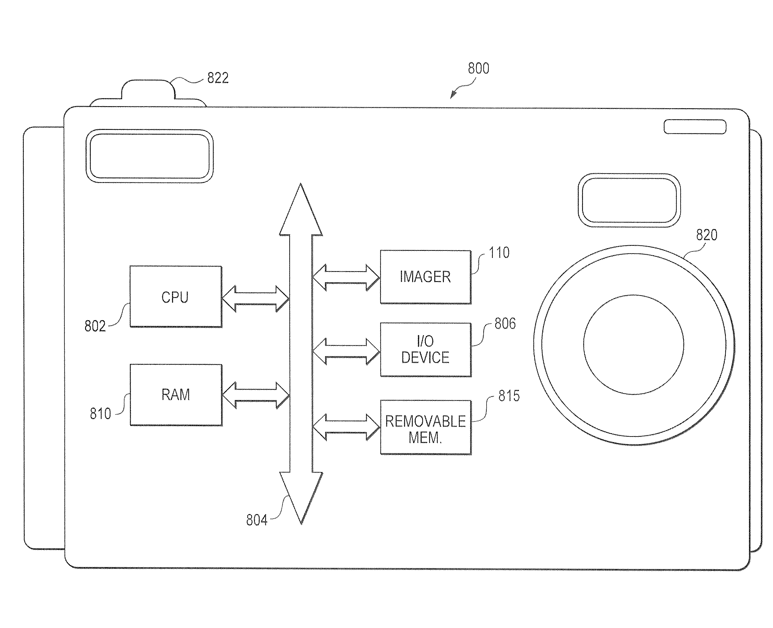
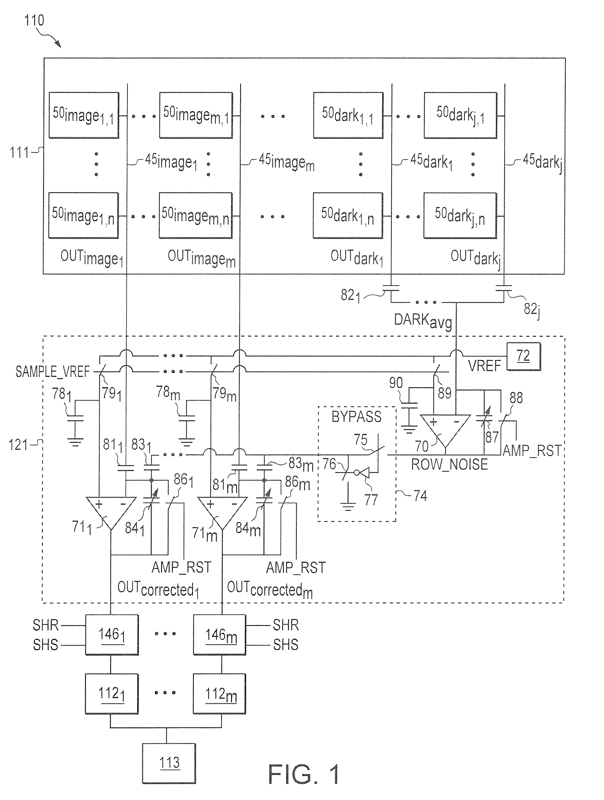
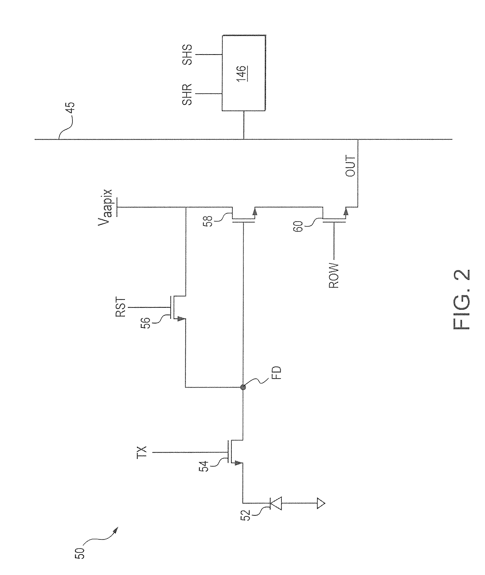
[0015]Method and apparatus embodiments described herein remove row noise and filter out hot pixels in the analog domain. Performing these functions in the analog domain allows imaging dies to be smaller and image processing to be faster and more accurate.

[0016]Imaging dies can be smaller because less dark reference pixels are required to accurately correct row noise in the analog domain (since row noise correction in the digital domain requires more dark references pixels to maintain accuracy because additional noise and signal modification is introduced during analog-to-digital conversion and subsequent processing). In addition, correcting row noise before analog gain reduces the number of dark reference pixels needed because row noise correction can be done independent of pixel color.

[0017]Image processing can be faster because row noise correction occurs during pixel sampling and the readout time is independent of the number of dark reference pixels. Image processing can also be ...


PUM


Abstract

An imaging device and method for operating the device. The imaging device comprises a pixel array that comprises a plurality of imaging pixels and dark reference pixels arranged in columns and rows. The dark reference pixels produce a noise signal that is subtracted from a pixel signal produced by the imaging pixels to correct row noise. In addition, the imaging device may comprise a hot pixel filtering circuit that blocks the output from hot pixels.

Description

FIELD OF THE INVENTION[0001]Embodiments of the invention are directed to analog processing of signals for an imager device.BACKGROUND OF THE INVENTION[0002]Solid state imaging devices, including charge coupled devices (CCD), complementary metal oxide semiconductor (CMOS) imaging devices, and others, have been used in photo imaging applications. A solid state imaging device circuit includes a focal plane array of pixel cells or pixels as an imaging sensor, each cell including a photosensor, which may be a photogate, photoconductor, a photodiode, or other photosensor having a doped region for accumulating photo-generated charge. For CMOS imaging devices, each pixel has a charge storage region, formed on or in the substrate, which is connected to the gate of an output transistor, typically a source follower transistor, which is part of a readout circuit. The charge storage region may be constructed as a floating diffusion region. In some CMOS imaging devices, each pixel may further inc...

Claims


Application Information

Patent Timeline
Patent Type & Authority Applications(United States)
IPC IPC(8): H04N9/64H04N5/335H04N5/361H04N5/367H04N5/378
CPCH04N5/3559H04N5/37457H04N5/367H04N5/361H04N25/59H04N25/63H04N25/68H04N25/778
Inventor MO, YAOWUXU, CHEN
Owner APTINA IMAGING CORP
Why Eureka
Try Eureka