Biasing system and method

a biasing system and biasing technology, applied in the field of memory devices, can solve the problems of unfavorable reducing the performance of the memory device, the thickness of the tunnel oxide in the high-voltage (hv) transistor may become so thin that it cannot reliably hold electrons on the floating gate of the cell, and the cell may not reliably store data

Active Publication Date: 2009-11-05
MICRON TECH INC
View PDF13 Cites 33 Cited by
  • Summary
  • Abstract
  • Description
  • Claims
  • Application Information

AI Technical Summary

Problems solved by technology

Unfortunately, as the cells and associated transistors are scaled, physical limitations may undesirably reduce the performance of the memory device.
For example, the memory cells and associated transistors are scaled, the tunnel oxide thickness in a high-voltage (HV) transistor may bec...

Method used


Image

  • Biasing system and method
  • Biasing system and method
  • Biasing system and method

Examples


Embodiment Construction

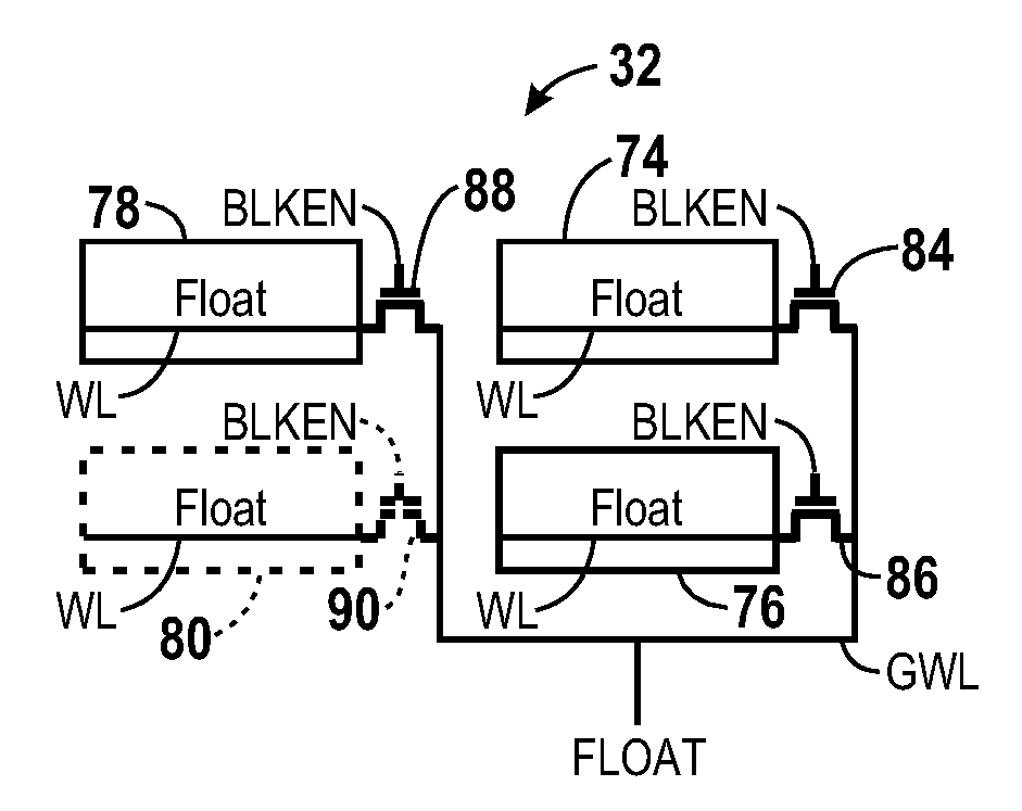
[0025]As discussed in further detail below, according to at least one embodiment of the present invention, the disclosed systems and methods relate to a biasing scheme for transistors of a memory device. More specifically, some embodiments include biasing local word lines during non-operational states. The biasing scheme in certain embodiments includes biasing a local word line to a voltage level that is not equal to a “negative” voltage supply (e.g., if the access devices connecting a global word line to a local word line are nMOS transistors, then the local word line would be biased above the negative supply voltage level, which is conventionally 0V). The biasing scheme is applied in a non-operation state, such as a stand-by state or active state prior to and / or after certain operation states (e.g., read, program, or erase states) of the memory device. Biasing the local word-line provides a bias voltage level that remains on the word line during the operations of the memory device...


PUM


Abstract

Embodiments are provided that include a memory system that includes a memory system, having an access device coupled between a global line and a local line and a voltage source coupled to the global line and configured to output a bias voltage on the global line when the memory system is in a non-operation state. The access device is selected when the memory system is in the non-operation state, and the access device is deselected when the memory system is in an other state. Further embodiments provide, for example, a method that includes coupling a global access line to a local access line, biasing the local access line to a voltage other than a negative supply voltage while a memory device is in a first state and uncoupling the global access line from the local access line while the memory device is in an other state.

Description

BACKGROUND[0001]1. Field of the Invention[0002]Embodiments of the invention relate generally to the field of memory devices and more particularly, to a system and method for biasing lines in semiconductor memories.[0003]2. Description of the Related Art[0004]Flash memory is a non-volatile memory that can be electrically erased and reprogrammed. It is primarily used in memory cards, USB flash drives, and the like, for storage of data in computer systems. Generally, flash memory stores information in an array of floating gate transistors, called “cells”, each of which traditionally stores one bit of information that is represented as a “0” or a “1”. The memory device often includes a grid-like arrangement of the cells and associated transistors. Each of the cells in the grid consumes a given amount of area and is spaced from one another by a generally uniform distance (e.g., pitch). Accordingly, the size and the pitch of the cells directly contribute to the overall size of the memory ...

Claims


Application Information

Patent Timeline
IPC IPC(8): G11C16/06
CPCG11C16/0483G11C16/30G11C16/10
Inventor TANZAWA, TORU
Owner MICRON TECH INC
Why Eureka
Try Eureka