Semiconductor memory device, operating method thereof, and compression test method thereof

a memory device and semiconductor technology, applied in the field of semiconductor memory devices, can solve the problems of ten million memory cell pass/fail test, limited and take a lot of test time to test memory cells, etc., to achieve the effect of maximizing the number of semiconductor memory devices that can be tested at a time and short tim

Inactive Publication Date: 2009-11-05
SK HYNIX INC
View PDF8 Cites 15 Cited by
  • Summary
  • Abstract
  • Description
  • Claims
  • Application Information

AI Technical Summary

Benefits of technology

[0040]Embodiments of the present invention are directed to providing a semiconductor memory device that can execute a compression test mode using a minimum number of input / output pads.
[0046]As the fabrication technologies of semiconductor memory devices are rapidly advanced, the integration density of the semiconductor memory devices increases so that ten millions of memory cells are integrated into a single semiconductor memory device. A compression test mode was proposed in order to test tens millions of memory cells in a short time. However, when storing the data in the banks in the compression test mode, the test operator must apply data to the respective input / output pads. In outputting the compressed data to the plurality of input / output pads, there is a limitation in the number of semiconductor memory devices that can be tested at a time according to the test pins of the test apparatus. In accordance with the invention, a minimum number of input / output pads can be used in the compression test mode. Therefore, the work efficiency is maximized because the data can be stored in the banks through a minimum number of input / output pads. Furthermore, data of various patterns can be stored in the banks even though a minimum number of input / output pads are used. Moreover, the number of the semiconductor memory devices that can be tested at a time is maximized because the compressed data can be output through a minimum number of input / output pads.

Problems solved by technology

However, it takes a lot of time to test the memory cells.
That is, a lot of test time is taken to determine pass / fail of ten millions of memory cells.
In addition, since a test apparatus having finite test pins must allocate four test pins per the semiconductor memory device, there is a limitation in the number of semiconductor memory devices that can be tested at a time.

Method used


Image

  • Semiconductor memory device, operating method thereof, and compression test method thereof
  • Semiconductor memory device, operating method thereof, and compression test method thereof
  • Semiconductor memory device, operating method thereof, and compression test method thereof

Examples


Embodiment Construction

[0059]Hereinafter, a semiconductor memory device, an operating method thereof, and a compression test method thereof in accordance with the present invention will be described in detail with reference to the accompanying drawings.

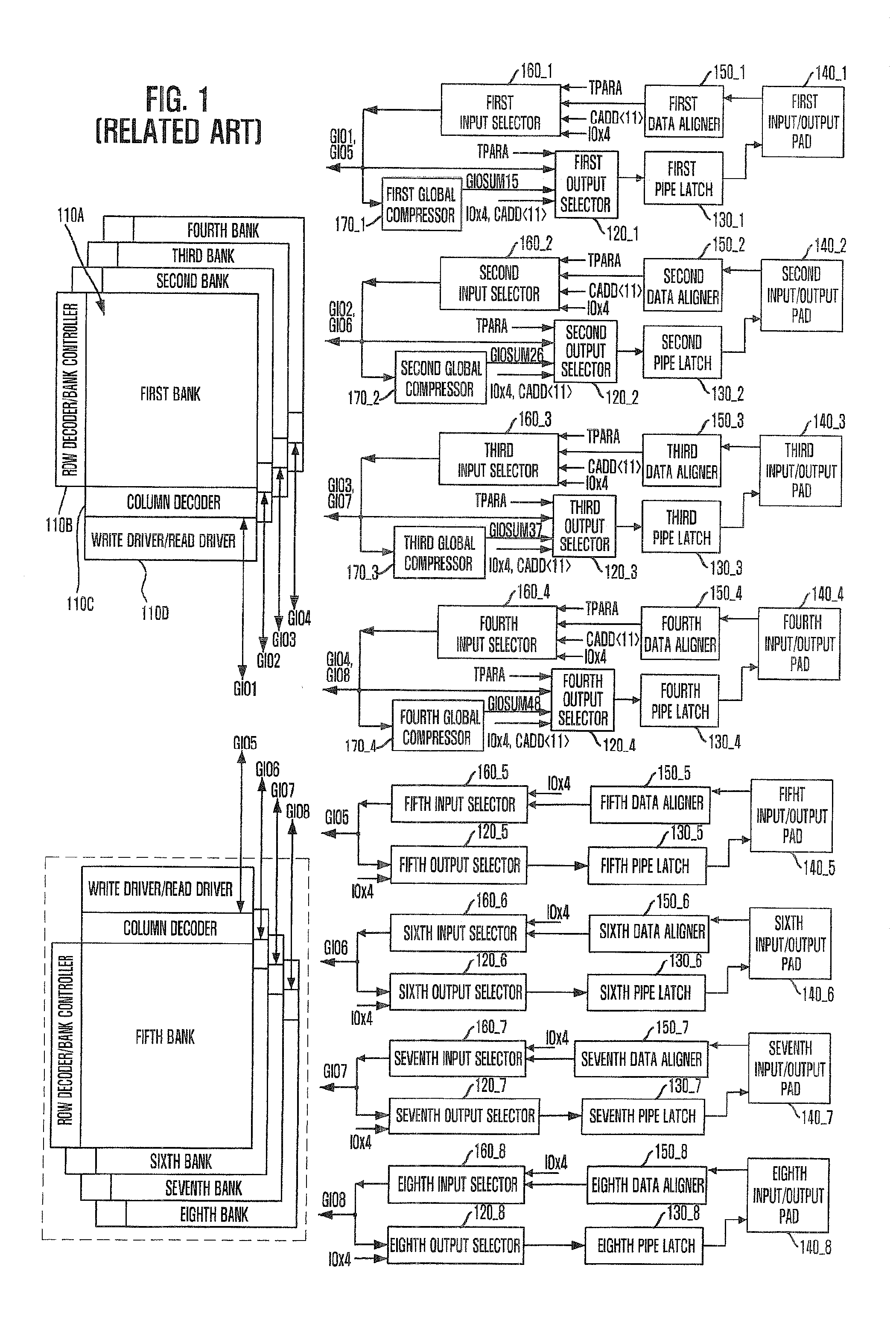
[0060]FIG. 4 is a block diagram of a semiconductor memory device in accordance with an embodiment of the invention. A DDR2 SDRAM is exemplarily illustrated in FIG. 4. The DDR2 SDRAM includes eight banks and eight input / output pads and can be set to x8 or x4 data width option. Also, since the DDR2 SDRAM uses a 4-bit prefetch scheme, each global input / output line includes four global input / output lines. That is, a first global input / output line GIO1 includes four global input / output lines GIO1, GIO1, GIO1 and GIO1. For convenience, the four global input / output lines GIO1, GIO1, GIO1 and GIO1 are indicated by one global input / output line GIO1. The number of the banks, the number of the input / output pads, and the number of the global input / output lines may be c...


PUM


Abstract

A semiconductor memory device including a plurality of banks, each including a plurality of memory cells, a pattern signal generator configured to generate pattern signals having combinations in response to an input signal applied through an arbitrary pad in a compression test mode. Input paths are configured to transfer the plurality of pattern signals to the corresponding banks.

Description

CROSS-REFERENCE TO RELATED APPLICATION[0001]The present invention claims priority of Korean patent application number 10-2008-0040830, filed on Apr. 30, 2008, which is incorporated by reference in its entirety.BACKGROUND OF THE INVENTION[0002]The present invention relates to a semiconductor design technology, and more particularly, to a semiconductor memory device having a compression test mode.[0003]As the fabrication technologies of semiconductor memory devices such as double data rate (DDR) synchronous dynamic random access memory (SDRAM) are rapidly advanced, the integration density of the semiconductor memory devices increases. Thus, ten millions of memory cells are integrated into a single semiconductor memory device. Due to the increase in the number of the memory cells, much more data can be stored. However, it takes a lot of time to test the memory cells. That is, a lot of test time is taken to determine pass / fail of ten millions of memory cells. The test time is an importa...

Claims


Application Information

Patent Timeline
Patent Type & Authority Applications(United States)
IPC IPC(8): G11C7/00G11C8/00
CPCG11C29/1201G11C2029/3602G11C29/36G11C7/10G11C29/00
Inventor SONG, SEONG-HWI
Owner SK HYNIX INC
Why Eureka
Try Eureka