EL display panel, electronic instrument and panel driving method

a technology of electronic instruments and display panels, applied in the direction of instruments, static indicating devices, etc., can solve the problems of gate-source voltage vgs appearing between the gate and the source electrode of the device driving transistor tb>2/b>, changes in the luminance of light emitted, etc., and achieve the effect of reducing the cost of manufacturing the driving circui

Inactive Publication Date: 2009-11-12
SONY CORP
View PDF10 Cites 23 Cited by
  • Summary
  • Abstract
  • Description
  • Claims
  • Application Information

AI Technical Summary

Benefits of technology

[0015]For the reasons described above, if a pixel circuit having the configuration shown in the circuit diagram of FIG. 4 is used, it is necessary to establish a driving method which is capable of giving a stable light emission characteristic independent of variations with the lapse of time and allows the organic EL display apparatus to be manufactured at a low cost.
[0017]In the case of this circuit configuration, a power-supply electric potential having two different magnitudes is shared by a plurality of power-supply lines, which compose a multi-consecutive-row bundle cited above, as a signal common to the power-supply lines. Thus, the number of output stages of a driving circuit for asserting the signal common to the power-supply lines pertaining to the multi-consecutive-row bundle can be reduced to a fraction of the number of output stages for a case in which a power-supply line is desired for driving pixel circuits provided on each matrix row. The reduction of the number of output stages allows the size of the driving circuit and the driving frequency to be also decreased as well. As a result, a low-cost driving circuit can be adopted in the organic EL display panel.
[0026]In the inventions proposed by the inventors of the present invention, power-supply lines each used for supplying a driving current to the organic EL light emitting device employed in a pixel circuit are driven by applying two or more electric potentials to the power-supply lines in multi-consecutive-row bundles each consisting of a plurality of adjacent power-supply lines stretched in the horizontal direction and tied to each other. Thus, the number of output stages of the driving circuit for asserting a power-supply electric potential on each of the multi-consecutive-row bundles can be reduced to a fraction of the number of output stages for a case in which a power-supply line is desired for driving pixel circuits provided on each matrix row. The reduction of the number of output stages allows the cost of manufacturing the driving circuit to be also decreased as well. As a result, a low-cost driving circuit can be adopted in the organic EL display panel.

Problems solved by technology

However, the pixel circuit having the configuration shown in the circuit diagram of FIG. 4 raises a problem that the gate-source voltage Vgs appearing between the gate and source electrodes of the device driving transistor T2 changes due to time-aging variations of the I-V characteristic of the organic EL light emitting device OLED.
The changes of the gate-source voltage Vgs appearing between the gate and source electrodes of the device driving transistor T2 cause driving-current variations which undesirably result in variations of the luminance of light emitted by the organic EL light emitting device OLED.

Method used


Image

  • EL display panel, electronic instrument and panel driving method
  • EL display panel, electronic instrument and panel driving method
  • EL display panel, electronic instrument and panel driving method

Examples


first embodiment

(B): First Embodiment

(B-1): System Configuration

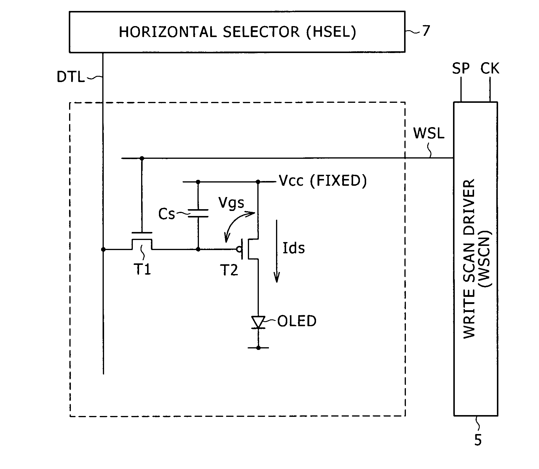
[0080]The following description explains a typical system configuration of the organic EL display panel 11 which is capable of getting rid of effects of characteristic variations exhibited by the device driving transistor T2 employed in the pixel circuit and capable of operating by making use of only few components composing the pixel circuit.

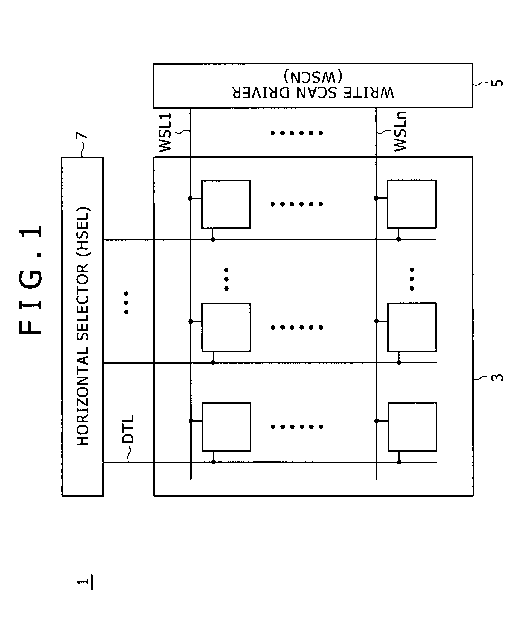
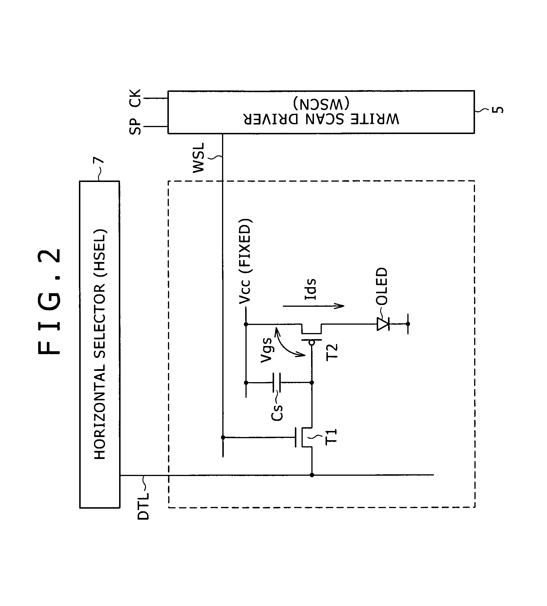
[0081]FIG. 6 is a block diagram showing a typical system configuration of the organic EL display panel 11 according to a first embodiment. The organic EL display panel 11 shown in the block diagram of FIG. 6 employs a pixel array section 21, a write scan driver 23, a power-supply line scan driver 25, a horizontal selector 27 and a time generator 29. Each of the write scan driver 23, the power-supply line scan driver 25 and the horizontal selector 27 serves as a driving circuit.

[0082]The pixel array section 21 has a matrix structure which is a matrix of sub-pixel circuits each located at the inters...

second embodiment

(C): Second Embodiment

(C-1): System Configuration

(a): Wiring Structure

[0109]The following description explains a wiring structure of the organic EL display panel and a driving method provided for the pixel circuit employed in the organic EL display panel. The wiring structure and the driving method are provided by a second embodiment and allow the cost of manufacturing the organic EL display panel to be reduced.

[0110]FIG. 18B is a diagram showing a wiring structure 31 of power-supply lines DSL employed in the pixel array section according to the second embodiment. By the way, for the purpose of comparison, FIG. 18A is given as a diagram showing a wiring structure of power-supply lines DSL employed in the pixel array section 21 according to the first embodiment.

[0111]In either of the wiring structures, a power-supply line DSL is stretched in the horizontal direction for every matrix row. In the case of the wiring structure shown in the diagram of FIG. 18A as the wiring structure of p...

third embodiment

(D): Third Embodiment

(D-1): System Configuration

[0142]FIG. 23 is a block diagram showing a typical system configuration of an organic EL display panel 51 according to a third embodiment. In the block diagram of FIG. 23, configuration elements identical with their respective counterparts shown in the diagram of FIG. 19 are denoted by the same reference numerals as the counterparts.

[0143]The organic EL display panel 51 shown in the block diagram of FIG. 23 employs a pixel array section 21, a write scan driver 23, a power-supply line scan driver 53, a horizontal selector 27 and a timing generator 35. Each of the write scan driver 23, the power-supply line scan driver 53 and the horizontal selector 27 serves as a driving circuit.

[0144]FIG. 24 is a block diagram showing connections between pixel circuits each serving as the circuit of a sub-pixel and the write scan driver 23, the power-supply line scan driver 53 as well as the horizontal selector 27 which are each used for driving the pi...


PUM


Abstract

Disclosed herein is an organic electro luminescence display panel provided with a pixel structure and a wiring structure which are adapted to an active matrix driving method; and driven by an electric potential asserted on each multi-consecutive-row bundle composed of adjacent power-supply lines, which are electrically tied to each other, each stretched in a horizontal direction and each used for supplying a driving current to an organic electro luminescence light emitting device employed in every pixel circuit of said organic electro luminescence display panel, to serve as an electric potential having two or more different magnitudes.

Description

BACKGROUND OF THE INVENTION[0001]1. Field of the Invention[0002]In general, the present invention explained in this invention specification relates to a driving technology for driving an organic EL (Electro Luminescence) display panel driven in accordance with control executed by adoption of an active matrix driving method. It is to be noted that the present invention proposed in this invention specification also has a mode of a driving method for driving the organic EL display panel and a mode of electronic instruments which each employ the organic EL display panel.[0003]2. Description of the Related Art[0004]FIG. 1 is a block diagram showing the general circuit configuration of an organic EL display panel 1 of an active matrix driving type. As shown in the block diagram of FIG. 1, the organic EL display panel 1 employs a pixel array section 3 as well as a write scan driver 5 and a horizontal selector 7, which are located in the peripheries of the pixel array section 3. Each of the...

Claims


Application Information

Patent Timeline
Patent Type & Authority Applications(United States)
IPC IPC(8): G09G3/30
CPCG09G3/3233G09G2300/0426G09G2300/043G09G2330/02G09G2300/0866G09G2320/043G09G2300/0842
Inventor YAMAMOTO, TETSUROUCHINO, KATSUHIDE
Owner SONY CORP
Why Eureka
Try Eureka