Board for display device and display device

a display device and display device technology, applied in the field of substrates for display devices and display devices, can solve the problems of low productivity, high cost, and loss of b>1/b>b, and achieve the effect of improving the performance of sealing the gap, enhancing the reliability of electrical connections, and securely achieving electrical connections

Inactive Publication Date: 2009-11-12
SHARP KK
View PDF3 Cites 11 Cited by
  • Summary
  • Abstract
  • Description
  • Claims
  • Application Information

AI Technical Summary

Benefits of technology

[0057]As described above, in the first invention, there are provided the convex portion having the configuration of a bank continuous or uncontinuous and a plurality of the independent concave portions arranged side by side or dotted between the display part to which the oriented film is applied and the position where the sealing compound is disposed. Therefore it is possible to securely prevent the applied oriented film from spreading to the position where the sealing compound is disposed. Thereby it is possible to prevent the contact between the oriented film and the sealing compound and seal the gap between the substrates opposed to each other.
[0058]In the second invention, between the display part and the electrode, there are provided the convex portion or / and a to plurality of the concave portions similar to those of the first invention. Therefore it is possible to prevent the applied oriented film from spreading to the electrode and securely connect the electrodes of a pair of the substrates opposed to each other via the conductive material when the substrates are disposed in confrontation. Thereby it is possible to enhance the reliability in the electrical connection.
[0059]In the third invention, the convex portion, the concave portion or / and the hole are formed on the distributing wire disposed on the substrate. Thereby the distributing wire is capable of restraining the oriented film from flowing without using a separate additional member, thus preventing the oriented film from reaching the position where the sealing compound is disposed.
[0060]The construction having all of the constituent features of the first, second, and third inventions is capable of preventing the oriented film applied to the display part from spreading to the position where the sealing compound is disposed and the position where the electrode is disposed, improving the performance of sealing the gap between the substrates opposed to each other, and securely accomplish the electrical connection between the electrodes of both substrates opposed to each other.

Problems solved by technology

Therefore it is very difficult to control the dimension of the outer edge of the display portion X when the resin solvent is applied.
Thus there is a fear that the resin solvent reaches the position where the sealing compound is disposed and the position where the common electrode 8 is disposed.
Thus the reliability in the performance of the oriented film in sealing the substrates 1A, 1B is lost.
When the groove 12a is formed deep to solve this problem, it is necessary to thick the organic insulation film 12, which leads to a high cost and a low productivity.

Method used


Image

  • Board for display device and display device
  • Board for display device and display device
  • Board for display device and display device

Examples


first embodiment

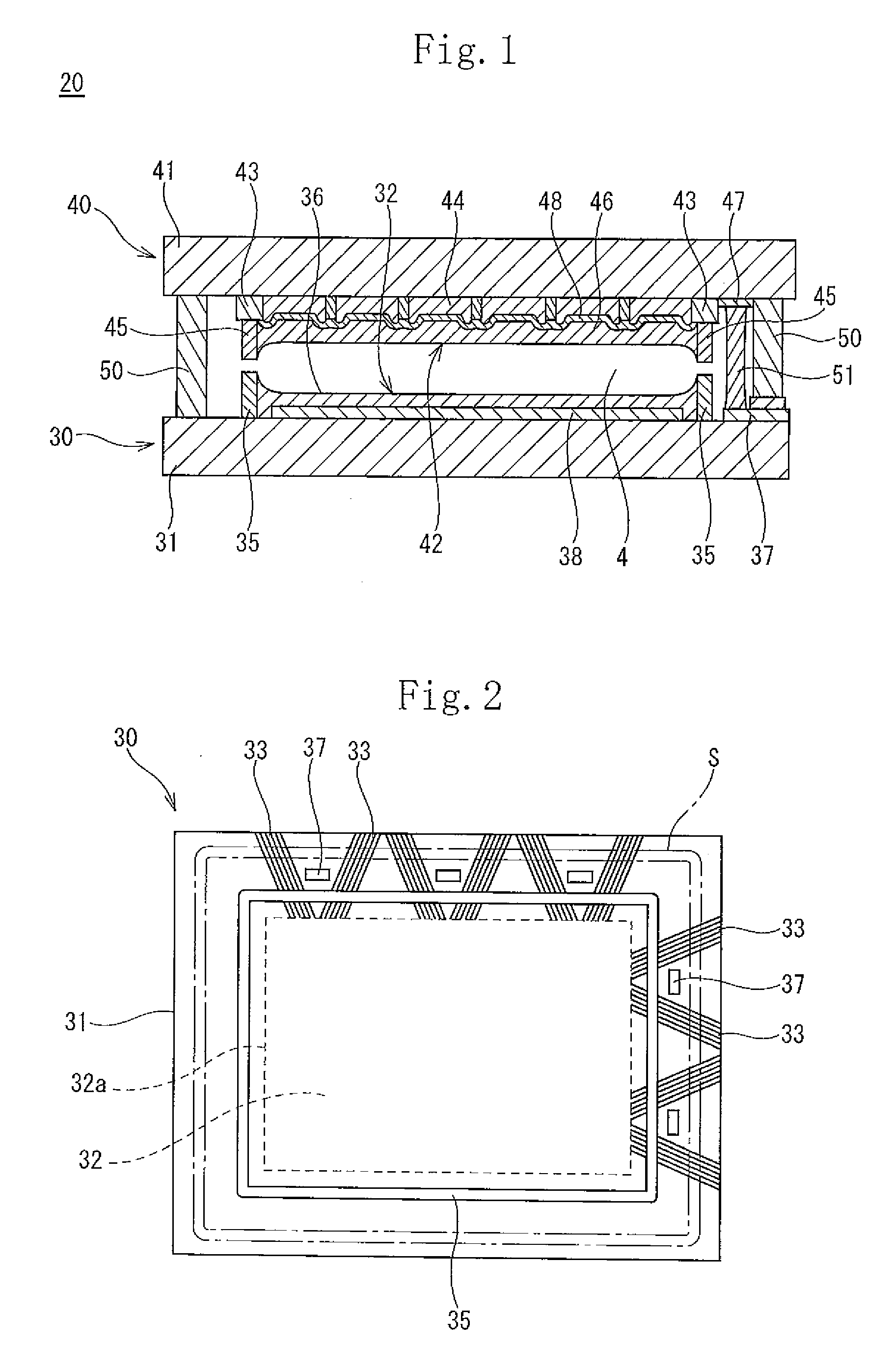
[0102]FIGS. 1 through 6 show the present invention. FIG. 1 shows a state in which a TFT array substrate 30 (hereinafter abbreviated as array substrate 30) and a color filter substrate 40 (hereinafter abbreviated as CF substrate 40) are combined with each other by opposing the array substrate 30 and the CF substrate 40 to each other with a liquid crystal of a liquid crystal display interposed therebetween.

[0103]The entire construction of the liquid crystal display is similar to that shown in FIG. 17. The array substrate 30 and the CF substrate 40 are disposed by opposing them to each other at a predetermined interval spaced from each other. A peripheral edge of the array substrate 30 and that of the CF substrate 40 are joined with each other via a sealing compound 50. A liquid crystal material 4 is enclosed in a space surrounded with the array substrate 30, the CF substrate 40, and the sealing compound 50.

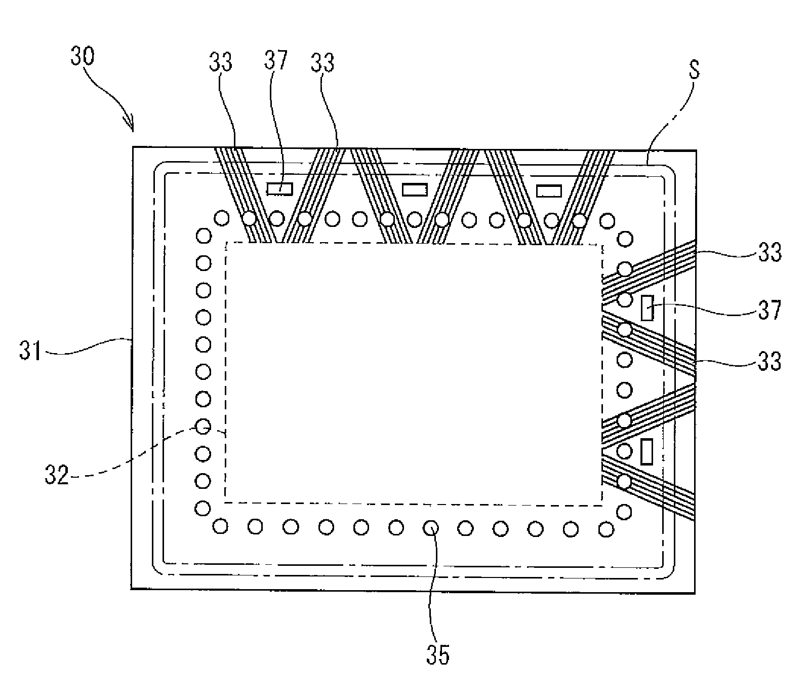
[0104]As shown in FIG. 2, in the array substrate 30, a central region of a glas...

second embodiment

[0141]FIGS. 12 and 13 show the present invention.

[0142]In the second embodiment, instead of the convex portions35, 45 formed on the array substrate 30 and the CF substrate 40 respectively, independent semicircular concave portions 60 (60a, 60b) and 61 (61a, 61b) are formed zigzag in two rows on the array substrate 30 and the CF substrate 40 respectively. More specifically, the concave portions 60a, 60b and the concave portions 61a, 61b are densely zigzag disposed at positions where a part of the concave portions 60a, 60b and the concave portions 61a, 61b overlap each other respectively.

[0143]In the concave portion 60 of the array substrate 30 shown in FIG. 12, between the outer edge 32a of the display part 32 and the region where the sealing compound 50 is disposed and in the portion where the common electrodes 37 are disposed, a resin film 62 is formed between the common electrodes 37 and the outer edge 32a of the display part 32. The concave portion 60 is formed on the resin film ...

third embodiment

[0154]FIG. 15 shows the present invention.

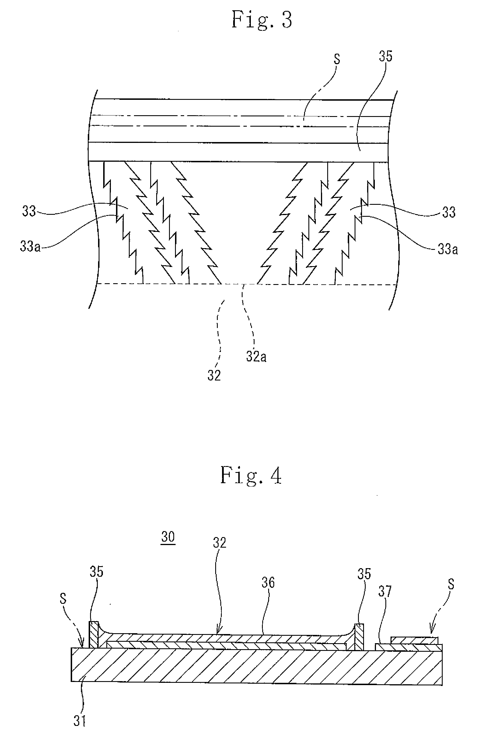
[0155]In the third embodiment, the bank-shaped convex portion 35 is formed on the array substrate 30, and an independent concave portion 60 is formed adjacently to the outer edge of the convex portion 35 at the side of the display part thereof.

[0156]The above-described construction is similar to a construction of a bank having a depth equal to the addition of the height of the convex portion 35 and the depth of the concave portion 60, thus securely intercepting the flow of the resin solvent forming the oriented film. Similarly to the array substrate 30, the CF substrate may be provided with the convex portion 35 and the concave portion 60 disposed adjacently thereto.

[0157]The third embodiment has the same construction as that of the first embodiment. Thus the same parts of the third embodiment as those of the first embodiment are denoted by the same reference numerals as those of the first embodiment, and description thereof is omitted herei...


PUM

PropertyMeasurementUnit
heightaaaaaaaaaa
heightaaaaaaaaaa
heightaaaaaaaaaa

Abstract

A substrate for a display having, on a surface thereof, a sealing compound disposed along a periphery of the substrate spaced at a predetermined interval from an outer edge of a display part to which an oriented film is applied; and a convex portion or / and a concave portion, for preventing the applied oriented film from spreading to the sealing compound, provided between the sealing compound and the outer edge of the display part. The convex portion has a configuration of a bank continuous or uncontinuous, whereas the concave portion is formed as a plurality of independent portions arranged side by side or dotted between the outer edge of the display part and the sealing compound.

Description

TECHNICAL FIELD[0001]The present invention relates to a substrate for a display and the display having the substrate. More particularly, in substrates preferably used as a TFT substrate and a color filter substrate opposed thereto with a liquid crystal interposed therebetween in a liquid crystal display, the present invention is intended to prevent the spread of an oriented film applied to a surface of the substrate so that the oriented film is prevented from reaching a sealing compound disposed on the periphery of a display part to seal the gap between the substrates and positions of electrodes mounted on the opposed substrates with the electrodes connected to each other.BACKGROUND ART[0002]In recent years, as a display such as monitors of televisions, personal computers, and the like, thin and flat FPD (Flat Panel Display) is frequently used. Of various kinds of the FPD, a plasma display and a liquid crystal display are mainly used.[0003]As shown in FIG. 16, in a color liquid crys...

Claims


Application Information

Patent Timeline
Patent Type & Authority Applications(United States)
IPC IPC(8): G02F1/1339
CPCG02F1/133711G02F2001/133354G02F1/1341G02F1/1339G02F1/133354
Inventor KOTANI, NAOKITAKAHASHI, KIMIO
Owner SHARP KK
Why Eureka
Try Eureka