Flex Circuit with Single Sided Routing and Double Sided Attach

a flex circuit and double-sided connection technology, applied in the direction of electrical apparatus construction details, instruments, conductive pattern formation, etc., can solve the problem of expensive manufacturing of one or more flex circuits, and achieve the effect of reducing the number of process steps and fabrication costs, reducing space consumption, and reducing the thickness of flex circuits

Active Publication Date: 2009-11-19
APPLE INC
View PDF28 Cites 60 Cited by
  • Summary
  • Abstract
  • Description
  • Claims
  • Application Information

AI Technical Summary

Benefits of technology

[0004]This relates to a flex circuit having conductive traces formed on only one side of a base film for attaching to both sides of a DITO touch sensor panel. By having conductive traces formed on only one side of the base film, the number of process steps and fabrication cost can be reduced because only a single etching step is needed. Furthermore, because the flex circuit is thinner, the resultant space savings can be utilized for other features in a device without enlarging the overall device package.
[0006]The flex circuit can include a first attachment area that can include active conductors and dummy conductors formed along its length for making electrical connections with pads on a top surface of the touch sensor panel. The flex circuit can also include a second attachment area that can include lower conductors formed at its distal ends for making electrical connections with pads on a bottom surface of the touch sensor panel. In some embodiments, lower conductors on the second attachment area are arranged in conjunction with active and dummy conductors on the first attachment area so that when the flex circuit is folded and bonded to the touch sensor panel, the lower conductors on the bottom surface of the touch sensor panel and the active and dummy conductors on the top surface are not on directly opposing sides of the touch sensor panel. This arrangement can minimize unwanted coupling of signals between the conductors.
[0007]All traces and conductors on the flex circuit can be formed on the same side of the flex circuit. Because the traces and conductors are formed on the same side of the flex circuit, no vias and plating are required, and a thinner flex circuit can be manufactured. As a result, a bend can be formed in the flex circuit with the very small radius required by the thinness of the touch sensor panel. The thinness of the flex circuit can have other advantages such as providing more room in the z-direction for other electronics and / or mechanical structures, or allowing for thinner overall devices. In addition, forming only a single layer of conductors and traces can reduce the number of process steps required (because only a single etching step is needed), which can reduce manufacturing costs.
[0008]In the first attachment area, a particular number of dummy conductors can be formed between the active conductors. The number of dummy conductors, and the spacing between the dummy conductors and the active conductors, can be chosen (e.g., empirically) in accordance with the type and thickness of the flex circuit and the cross-sectional dimensions of the conductors. By the proper selection of conductor spacing, enough space can remain between the conductors (dummy and active) to retain most of the ACF underneath the first attachment area, minimizing the amount of ACF that is squeezed out.
[0010]To provide enhanced shielding for the single-sided flex circuits, thin conductive films can be attached to both sides of the flex circuits. The flex circuit can include a base film upon which a layer of conductive traces (e.g. copper) and an insulator can be formed. One or more conductive traces can be held at a fixed potential (e.g. ground). In one embodiment, a first opening (or notch) in the insulator can be formed over a particular conductive trace that is held at a fixed potential such as ground. Conductive film can then be applied over the insulator, where it can conform to the shape of the opening and make electrical contact with one or more of the fixed potential traces to hold the conductive film at the fixed potential. When the conductive film is held at the fixed potential, it can serve as a shield for the conductive traces.

Problems solved by technology

However, it can be expensive to manufacture the one or more flex circuits that are required to provide off-board connectivity for the drive and sense lines.

Method used


Image

  • Flex Circuit with Single Sided Routing and Double Sided Attach
  • Flex Circuit with Single Sided Routing and Double Sided Attach
  • Flex Circuit with Single Sided Routing and Double Sided Attach

Examples


Embodiment Construction

[0029]In the following description of preferred embodiments, reference is made to the accompanying drawings which form a part hereof, and in which it is shown by way of illustration specific embodiments in which the invention can be practiced. It is to be understood that other embodiments can be used and structural changes can be made without departing from the scope of the embodiments of this invention.

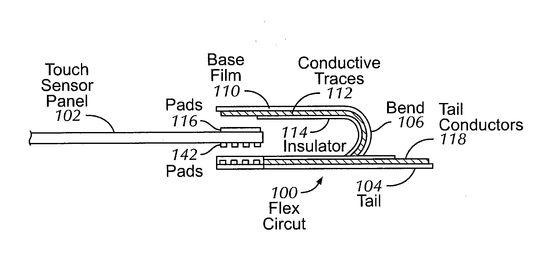
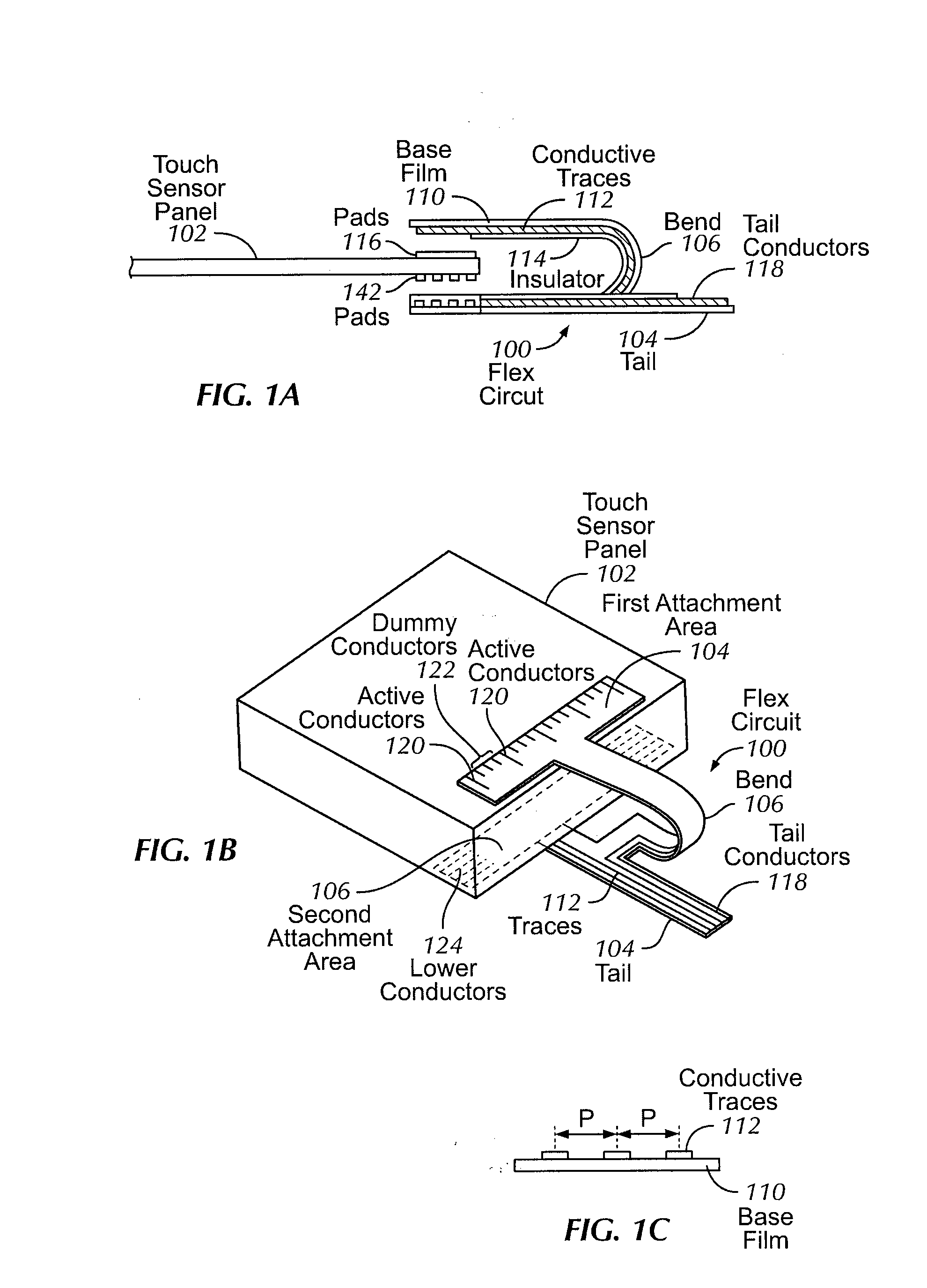
[0030]This relates to a flex circuit having conductive traces formed on only one side of a base film for attaching to both sides of a DITO touch sensor panel. By having conductive traces formed on only one side of the base film, the number of process steps and fabrication cost can be reduced because only a single etching step is needed. Furthermore, because the flex circuit is thinner, the resultant space savings can be utilized for other features in a device without enlarging the overall device package.

[0031]Although embodiments of the invention may be described and illustrated here...


PUM

PropertyMeasurementUnit
conductiveaaaaaaaaaa
flexibleaaaaaaaaaa
areaaaaaaaaaaa

Abstract

A flex circuit having conductive traces formed on only one side of a base film for attaching to both sides of a DITO touch sensor panel is disclosed. By having conductive traces formed on only one side of the base film, the number of process steps and fabrication cost can be reduced because only a single etching step is needed. Furthermore, because the flex circuit is thinner, the resultant space savings can be utilized for other features in a device without enlarging the overall device package.

Description

FIELD OF THE INVENTION[0001]This relates generally to touch sensor panels, and more particularly, to cost-effective flex circuit designs capable of being attached to both sides of a touch sensor panel.BACKGROUND OF THE INVENTION[0002]Many types of input devices are presently available for performing operations in a computing system, such as buttons or keys, mice, trackballs, joysticks, touch sensor panels, touch screens and the like. Touch screens, in particular, are becoming increasingly popular because of their ease and versatility of operation as well as their declining price. Touch screens can include a touch sensor panel, which can be a clear panel with a touch-sensitive surface, and a display device such as a liquid crystal display (LCD) that can be positioned partially or fully behind the panel so that the touch-sensitive surface can cover at least a portion of the viewable area of the display device. Touch screens can allow a user to perform various functions by touching the...

Claims


Application Information

Patent Timeline
Patent Type & Authority Applications(United States)
IPC IPC(8): H05K1/03H05K3/00
CPCH05K2201/053H05K2201/09781H05K1/147Y10T156/1052H05K3/361Y10T29/49155H05K2203/1572Y10T156/10H05K1/118G06F3/0416Y10T29/49124H05K3/323G06F2203/04103G06F3/04164
Inventor GRUNTHANER, MARTIN PAUL
Owner APPLE INC
Why Eureka
Try Eureka