Solid-state image sensor, solid-state image sensing device, and method of producing the same

a solid-state image and sensor technology, applied in the direction of transistors, television systems, radio control devices, etc., can solve the problem of limit in increasing the ratio of the surface area of the light receiving portion (photodiodes) to the area of one pixel, and achieve the effect of increasing the ratio of the surface area and reducing the occupation area of the read channel

Inactive Publication Date: 2009-11-19
UNISANTIS ELECTRONICS SINGAPORE PTE LTD
View PDF7 Cites 14 Cited by
  • Summary
  • Abstract
  • Description
  • Claims
  • Application Information

AI Technical Summary

Benefits of technology

[0010]As described above, in the conventional solid-state image sensors, the photodiode (PD), the read channel, n-type CCD channel region, and the p+-type isolation region are formed in a plane, and thus there has been a limitation in increasing a ratio of a surface area of the light receiving portion (photodiode) to an area of one pixel. Therefore, it is an object to provide a CCD solid-state image sensor, in which an area of the read channel is reduced, and the ratio of the surface area of the light receiving portion (photodiode) to the area of one pixel is increased.
[0025]The photo diode (PD), the read channel, the n type CCD channel region, and the p+-type isolation region are formed in a plain face, and thus there has been a limitation in increasing the ratio of the surface area of the light receiving (photo diode) to the area of one pixel, in the conventional CCD solid-state image sensor, but according to the present invention, it is possible to provide the CCD solid-state image sensor, in which an occupation area of the read channel can be greatly reduced by arranging the read channel non-horizontally, and the ratio of the surface area of the light receiving portion (photodiode) to the area of one pixel is increased.

Problems solved by technology

As described above, in the conventional solid-state image sensors, the photodiode (PD), the read channel, n-type CCD channel region, and the p+-type isolation region are formed in a plane, and thus there has been a limitation in increasing a ratio of a surface area of the light receiving portion (photodiode) to an area of one pixel.

Method used


Image

  • Solid-state image sensor, solid-state image sensing device, and method of producing the same
  • Solid-state image sensor, solid-state image sensing device, and method of producing the same
  • Solid-state image sensor, solid-state image sensing device, and method of producing the same

Examples


Embodiment Construction

[0073]Hereinafter, embodiments of the present invention will be described in detail with reference to the accompanying drawings.

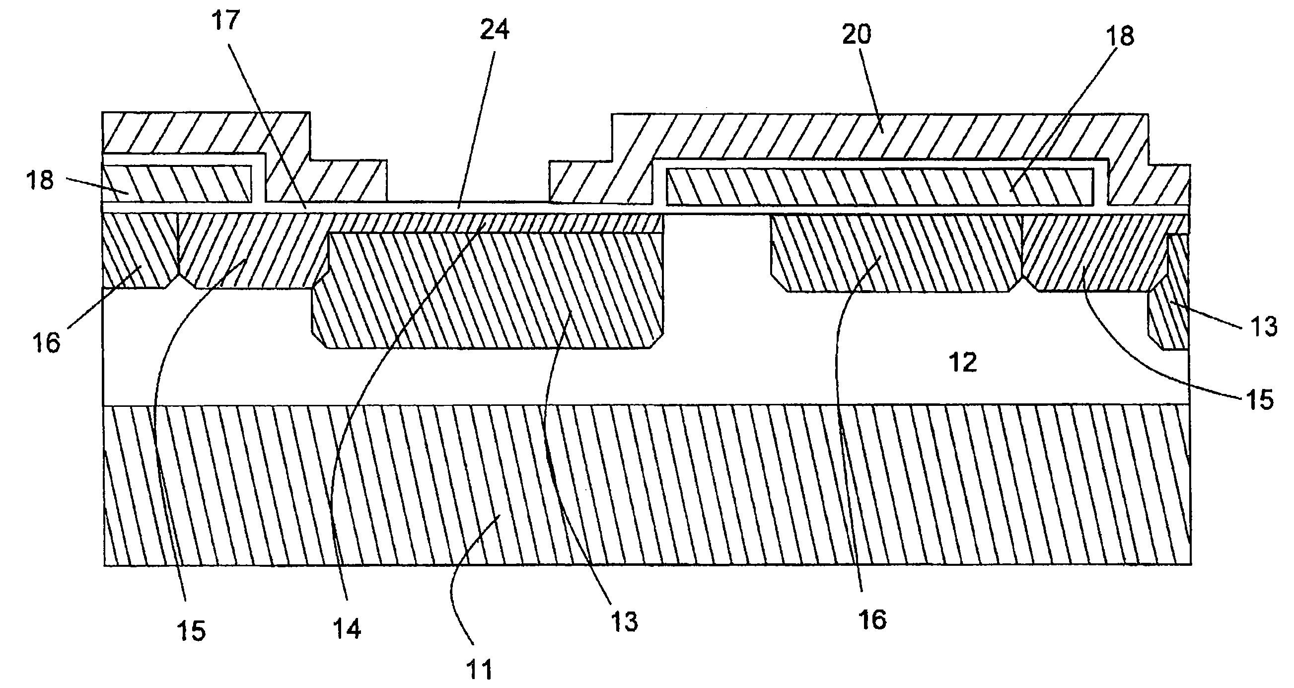
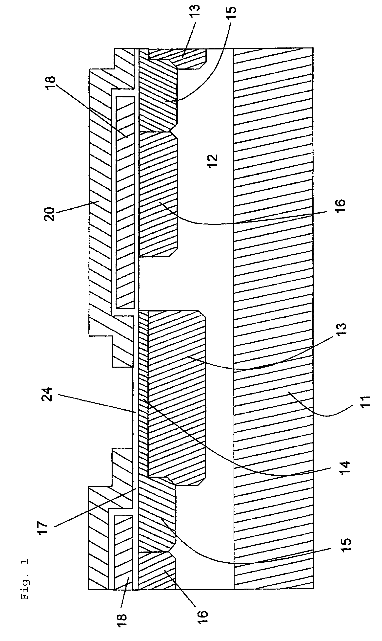
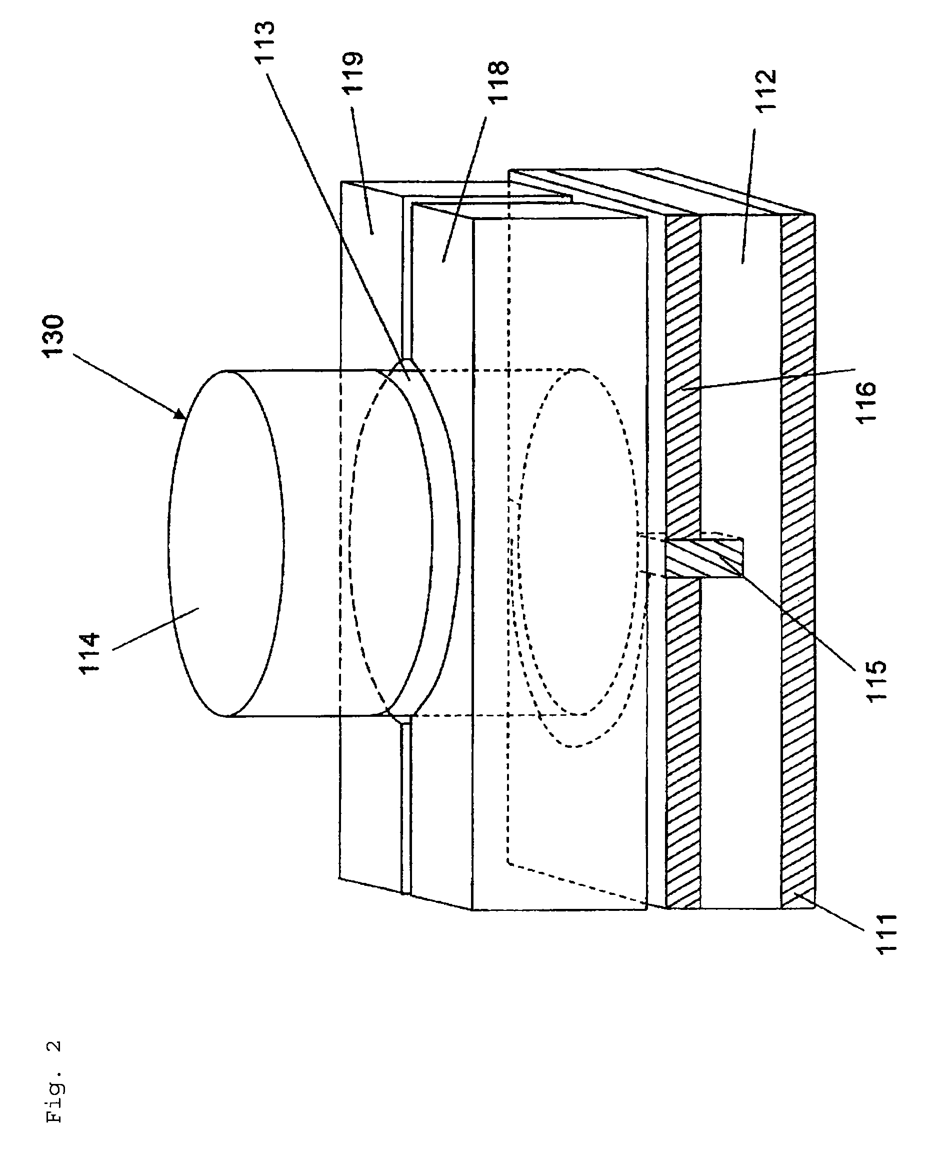
[0074]FIGS. 2 and 3 show a perspective view and a plan view of one CCD solid-state image sensor according to a first embodiment of the present invention, respectively. FIG. 4 is a cross-sectional view taken from line X1-X1′ shown in FIG. 3, and FIG. 5 is a cross-sectional view taken from line Y1-Y1′ shown in FIG. 3.

[0075]A p-type well region 112 is formed on an n-type substrate 111, and a p-type pillar-shaped semiconductor layer 131 is further formed on the p-type well region 112. An n-type photoelectric conversion region 113 in which an amount of charge is changed by light is formed on the top of the p-type pillar-shaped semiconductor layer 131, and a p+-type region 114 is further formed on the surface of the n-type photoelectric conversion region 113, while being spaced apart from the top end of the p-type pillar-shaped semiconductor layer 131 by a predet...


PUM


Abstract

It is an object to provide a CCD solid-state image sensor, in which an area of a read channel is reduced and a rate of a surface area of a light receiving portion (photodiode) to an area of one pixel is increased. There is provided a solid-state image sensor, including: a first conductive type semiconductor layer; a first conductive type pillar-shaped semiconductor layer formed on the first conductive type semiconductor layer; a second conductive type photoelectric conversion region formed on the top of the first conductive type pillar-shaped semiconductor layer, an electric charge amount of the photoelectric conversion region being changed by light; and a high-concentrated impurity region of the first conductive type formed on a surface of the second conductive type photoelectric conversion region, the impurity region being spaced apart from a top end of the first conductive type pillar-shaped semiconductor layer by a predetermined distance, wherein a transfer electrode is formed on the side of the first conductive type pillar-shaped semiconductor layer via a gate insulating film, a second conductive type CCD channel region is formed below the transfer electrode, and a read channel is formed in a region between the second conductive type photoelectric conversion region and the second conductive type CCD channel region.

Description

RELATED APPLICATIONS[0001]This application is a continuation of PCT / JP2007 / 074961, filed on Dec. 26, 2007. The entire content of this application is incorporated herein by reference.BACKGROUND OF THE INVENTION[0002]The present invention relates to a solid-state image sensor, a solid-state image sensing device, and a method of producing the same, and in particular, to a CCD solid-state image sensor, a CCD solid-state image sensing device, and a method of producing the same.[0003]A conventional solid-state image sensor used in a video camera or the like, in which light sensing elements are arranged in matrix form, includes, between light sensing element lines, a vertical charge coupled device (Vertical CCD: Charge Coupled Device) for reading signal charges generated by the light sensing element lines.[0004]A structure of the aforementioned conventional solid-state image sensor will be described in the following (refer to, for example, Patent Document 1). FIG. 1 is a sectional view sho...

Claims


Application Information

Patent Timeline
Patent Type & Authority Applications(United States)
IPC IPC(8): H01L27/148H01L31/18H04N5/335H04N5/369H04N5/372
CPCH01L27/14812H01L27/14837Y02E10/50H01L31/03529H01L31/035281H01L27/146
Inventor MASUOKA, FUJIONAKAMURA, HIROKI
Owner UNISANTIS ELECTRONICS SINGAPORE PTE LTD
Why Eureka
Try Eureka