Semiconductor device and manufacturing method for semiconductor device

a semiconductor device and semiconductor technology, applied in semiconductor devices, semiconductor/solid-state device details, electrical apparatus, etc., can solve the problems of high cost, large number of steps, and time-consuming thick plating, so as to suppress and reduce the overall height of the pop-type semiconductor device

Inactive Publication Date: 2009-11-19
PANASONIC CORP
View PDF13 Cites 23 Cited by
  • Summary
  • Abstract
  • Description
  • Claims
  • Application Information

AI Technical Summary

Benefits of technology

[0033]Hence, the sealing resin is formed using a compression molding method while the respective front surfaces of the plurality of platform electrodes are pressed against the release sheet possessing flexibility and elasticity. Therefore, the sealing resin can be formed into a structure in which the platform electrodes are exposed at the bottom of the recess portion easily. Moreover, the sealing resin is formed when the parts corresponding to the plurality of platform electrodes are removed, thereby eliminating the need to perform deburring and cleaning on the sealing resin after the seal is formed.
[0034]According to the present invention, the plurality of projecting electrodes of the other semiconductor device can be dropped into the recess portion formed in the sealing resin, and as a result, the overall height of the PoP type semiconductor device can be suppressed. The reason for this is that when the PoP type semiconductor device is constructed, the plurality of projecting electrodes of the other semiconductor device are inserted in alignment with the recess portion and fixed on the plurality of front surface lands or the plurality of platform electrodes disposed at the bottom of the recess portion, and therefore the effect of the height of the plurality of projecting electrodes of the other semiconductor device on the overall height of the PoP type semiconductor device can be reduced.
[0035]Further, the sealing resin is formed using a compression molding method while the respective front surfaces of the plurality of front surface lands or the plurality of platform electrodes are pressed against the release sheet possessing flexibility and elasticity. Therefore, the sealing resin can be formed into a structure in which the plurality of front surface lands or the plurality of platform electrodes are exposed at the bottom of the recess portion easily. Moreover, the sealing resin is formed when the parts corresponding to the plurality of front surface lands or the plurality of platform electrodes are removed, thereby eliminating the need to perform deburring and cleaning on the sealing resin after a seal is formed.
[0036]The present invention may be used as a semiconductor device on which another semiconductor device can be stacked or the like, and more particularly as a semiconductor device or the like with which a PoP type semiconductor device can be constituted easily and at low cost, and in which the reliability of a joint part between the semiconductor device and another semiconductor device is high.

Problems solved by technology

First, in the semiconductor device according to the first example, the surface area of the post portion increases toward the front surface of the sealing resin, and it is therefore difficult to form the post portion using multiple pins at a narrow pitch. Moreover, the number of steps is large, thick plating takes time, and cost is high.
In the semiconductor device according to the second example, when a plurality of similar semiconductor devices are stacked, the mounting height increases in proportion to the height of a projecting electrode of the stacked similar semiconductor devices, and as a result, a reduction in height cannot be achieved.
In the semiconductor device according to the third example, a similar problem to that of the semiconductor device according to the second example occurs, and in addition, an increase in cost occurs for formation of the wiring in the thickness direction of the sealing resin layer.

Method used


Image

  • Semiconductor device and manufacturing method for semiconductor device
  • Semiconductor device and manufacturing method for semiconductor device
  • Semiconductor device and manufacturing method for semiconductor device

Examples


first embodiment

[0064]A first embodiment of the present invention will be described below.

[0065](Constitution)

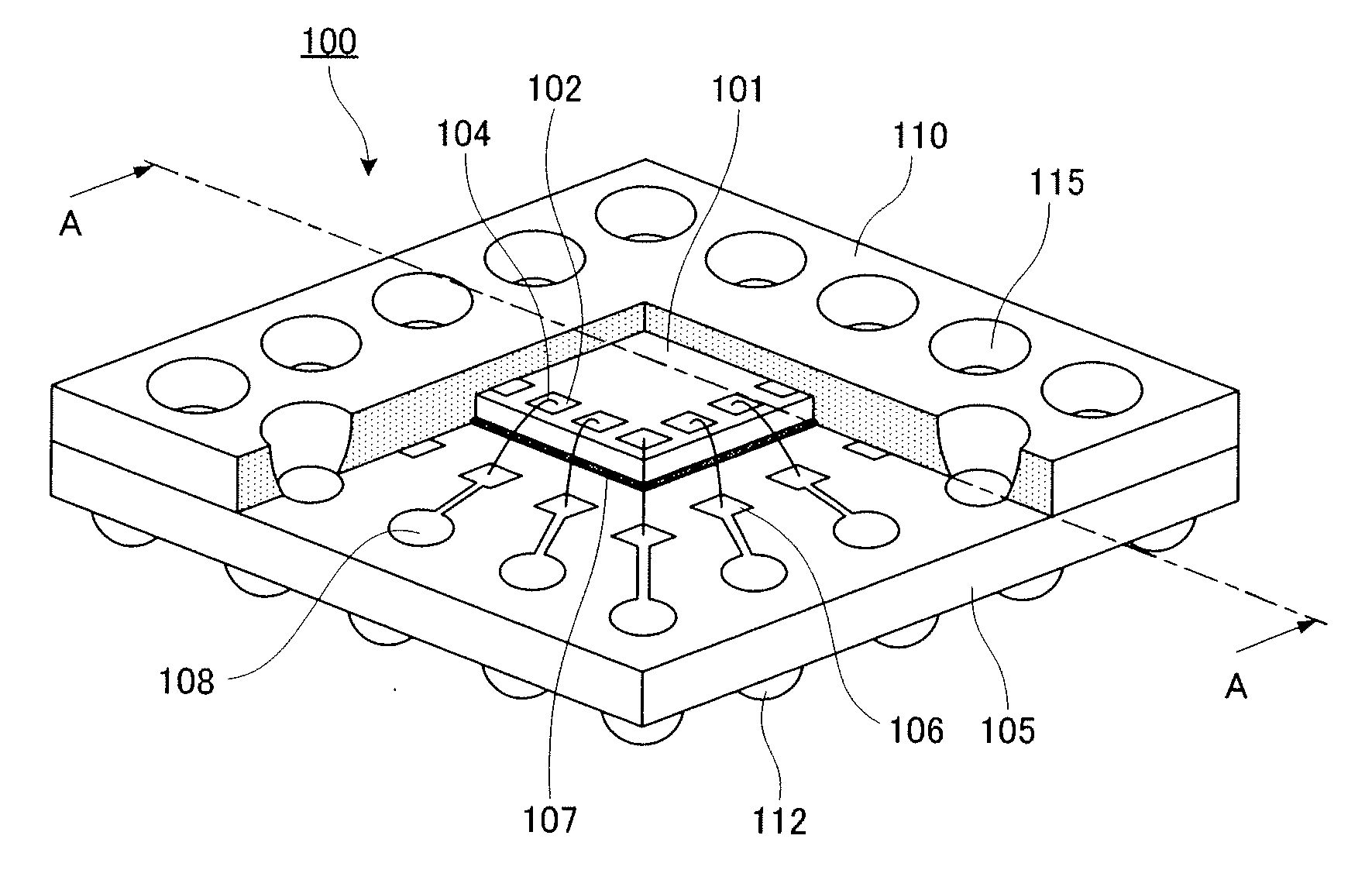
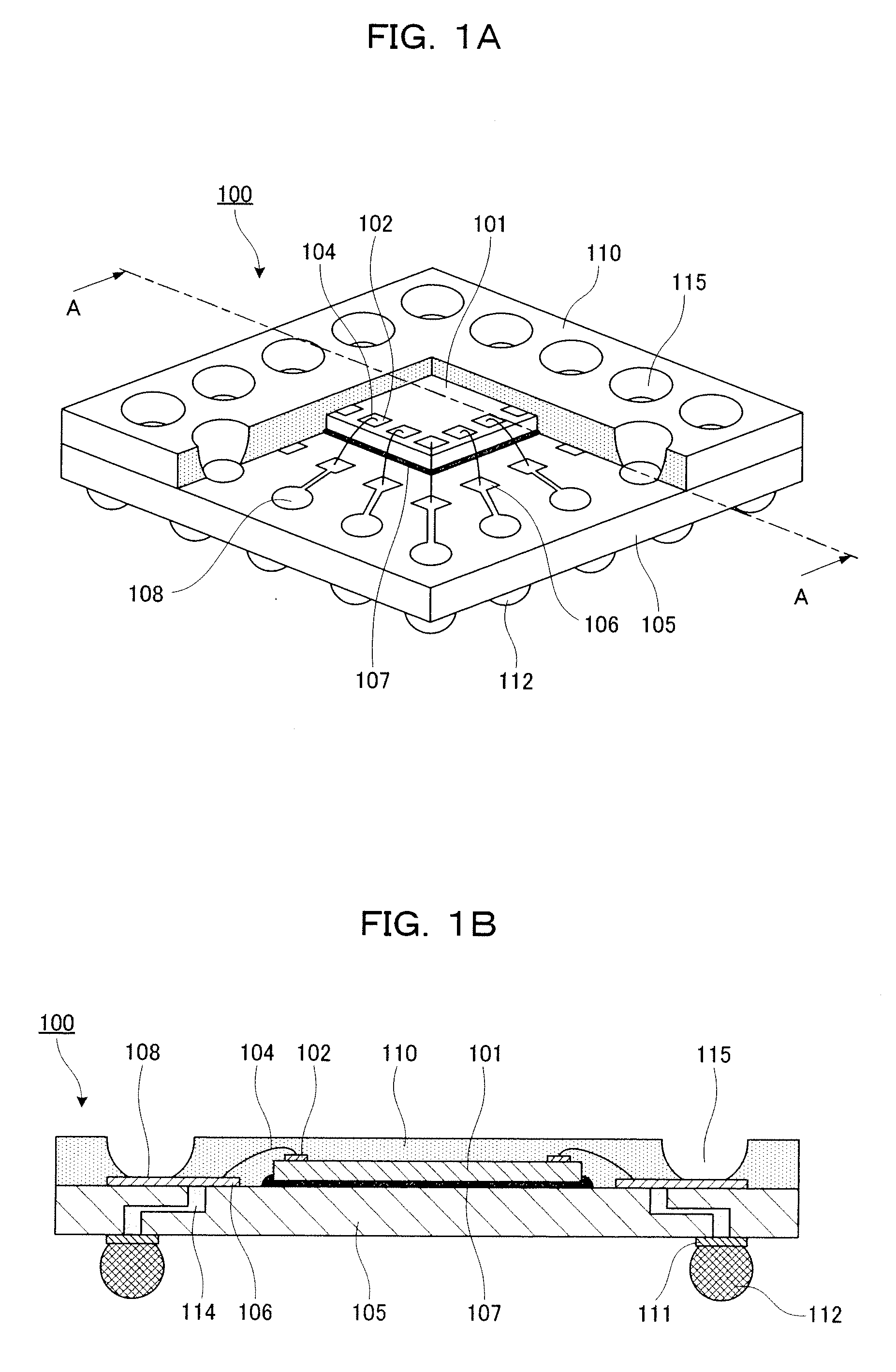
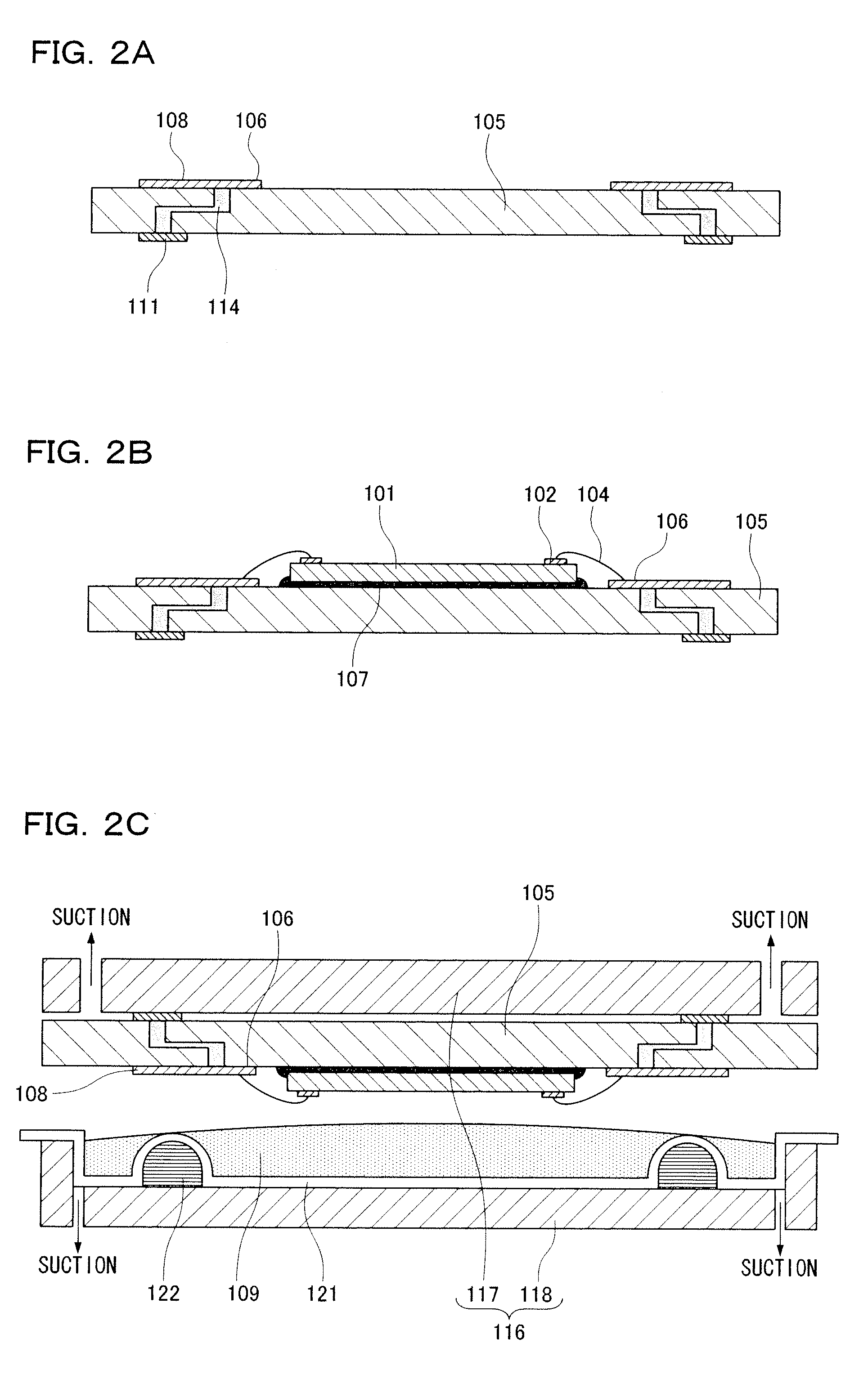
[0066]First, the constitution of a semiconductor device according to this embodiment will be described. Note that for convenience, the thickness, length, number of electrodes, and so on of the various members shown in the drawings differ from reality.

[0067]As shown in FIGS. 1A and 1B, a semiconductor device 100 is a semiconductor device on which another semiconductor device can be stacked. In this example, the semiconductor device 100 includes a semiconductor chip 101, a wiring board 105, a sealing resin 110, and a plurality of projecting electrodes 112.

[0068]Note that in FIG. 1A, a part of the sealing resin 110 has been removed to make the structure of the semiconductor device 100 easier to see.

[0069](Semiconductor Chip 101)

[0070]The semiconductor chip 101 includes an integrated circuit (not shown) and a plurality of electrode terminals 102. Taking the side on which the plurality of electr...

second embodiment

[0118]A second embodiment of the present invention will be described below.

[0119](Constitution)

[0120]First, the constitution of a semiconductor device according to this embodiment will be described. Note that identical constitutional elements to the first embodiment have been allocated identical reference numerals, and description thereof has been omitted.

[0121]As shown in FIGS. 5A and 5B, a semiconductor device 200 differs from the semiconductor device 100 according to the first embodiment on the following points (1) and (2).

[0122]Note that in FIG. 5A, a part of an elevated electrode 209 and a sealing resin 210 has been removed to make the structure of the semiconductor device 200 easier to see.

[0123](1) A plurality of platform electrodes 209 corresponding respectively to the plurality of front surface lands 108 to form pairs therewith are formed respectively on the front surface lands 108.

[0124]Here, the plurality of platform electrodes 209 are formed on the front surface lands 10...

third embodiment

[0159]A third embodiment of the present invention will be described below. Note that identical constitutional elements to the first embodiment have been allocated identical reference numerals, and description thereof has been omitted.

[0160](Constitution)

[0161]As shown in FIG. 8, a semiconductor device 300 differs from the semiconductor device 100 according to the first embodiment in that a semiconductor chip 301 is mounted on a wiring board 305 by a flip chip method.

[0162]The semiconductor chip 301 includes a plurality of bumps 323 instead of the plurality of electrode terminals 102 of the first embodiment. Here, the plurality of bumps 323 are disposed on a rear surface of the semiconductor chip 301 and electrically connected to an integrated circuit (not shown).

[0163]The wiring board 305 includes a plurality of semiconductor chip lands 328 instead of the plurality of connection terminals 106 of the first embodiment. Here, the plurality of semiconductor chip lands 328 are disposed i...


PUM


Abstract

A semiconductor device comprises: (a) a wiring board having front surface lands disposed on a front surface and rear surface lands disposed on a rear surface; (b) a semiconductor chip formed with an integrated circuit and electrode terminals electrically connected to the integrated circuit; and (c) a sealing resin that covers a front side of the wiring board when the semiconductor chip is mounted on the front side of the wiring board such that the front surface lands and the rear surface lands are electrically connected to the electrode terminals, wherein (d) holes having a shape and dimensions that allow projecting electrodes of the other semiconductor device to be inserted therein are formed in the sealing resin such that the front surface lands disposed further toward an inner side than a front surface of the semiconductor chip are exposed.

Description

BACKGROUND OF THE INVENTION[0001]1. Field of the Invention[0002]The present invention relates to a semiconductor device on which another semiconductor device can be stacked, and more particularly to a semiconductor device with which a PoP type semiconductor device can be constructed easily and at low cost and in which the reliability of a joint part between the semiconductor device and another semiconductor device is high.[0003]2. Description of the Related Art[0004]Conventionally, a Package on Package type (to be referred to hereafter as a “PoP type”) semiconductor device is used in cellular telephones, digital cameras, portable personal computers, and so on. A semiconductor device suitable for three-dimensional mounting is used in a PoP type semiconductor device. Various semiconductor devices in which an upper portion of a projecting electrode used for lamination purposes is exposed have been proposed as a semiconductor device suitable for three-dimensional mounting.First Example[...

Claims


Application Information

Patent Timeline
Patent Type & Authority Applications(United States)
IPC IPC(8): H01L23/04H01L21/00
CPCH01L21/565H01L2225/1088H01L23/3128H01L25/105H01L2224/16145H01L2224/16225H01L2224/32225H01L2224/48091H01L2224/48227H01L2224/49171H01L2224/73207H01L2224/73265H01L2225/0651H01L2225/06513H01L2924/15192H01L2924/15311H01L2924/15331H01L2924/1815H01L21/566H01L2225/1023H01L2924/0132H01L24/48H01L24/49H01L2924/01079H01L2924/01322H01L2924/3511H01L2224/45124H01L2224/45139H01L2224/45144H01L2224/45147H01L2924/01047H01L2924/12041H01L24/45H01L2225/1058H01L2924/00014H01L2924/00H01L2924/00012H01L24/73H01L2224/05554H01L2224/45015H01L2924/14H01L2924/15174H01L2924/181H01L2924/20751H01L2924/20752H01L2924/20753H01L2924/20754
Inventor YAMADA, YUICHIRO
Owner PANASONIC CORP
Why Eureka
Try Eureka