Method of maintaining photolithographic precision alignment after wafer bonding process

a technology of photolithographic precision and bonding process, which is applied in the direction of instruments, optical elements, mountings, etc., can solve the problems of reducing affecting the performance of the device, and affecting the alignment accuracy of the wafer, so as to achieve the effect of easy exposure and upgrade the alignment precision

Inactive Publication Date: 2005-11-22
ASIA PACIFIC MICROSYST
View PDF6 Cites 14 Cited by
  • Summary
  • Abstract
  • Description
  • Claims
  • Application Information

AI Technical Summary

Benefits of technology

[0013]It is an object of the present invention to provide a method of maintaining photolithographic precision alignment for a wafer after it is bonded. The method is performed by etching two cavities on the top wafer at the position corresponding to an alignment marks made on the bottom wafer, afterwards the bonded the top and the bottom wafers are treated with high temperature annealing process and thinning process by grinding the top wafer so as to form a membrane of wafer structure until the alignment marks made on the bottom wafer is exposed. Since the photolithographic process is carried out for both top and bottom wafer structure with respect to this alignment marks so that the exposure alignment equipment does not need double sides alignment capability for performing photolithography.
[0014]It is another object of the present invention to provide a method of maintaining photolithographic precision alignment for a wafer after being bonded that the alignment marks made on the bottom wafer can be exposed easily from the slot of the top wafer so as to upgrade the alignment precision between the top and the bottom wafers.
[0015]It is one more object of the present invention to provide a method of maintaining photolithographic precision alignment for a wafer after being bonded that by means of easily exposing this alignment marks from the cavities of the top wafer so as to provide a suspension membrane element for aligning a top structure with a bottom structure of devices such as a pressure sensor, an angular rate sensor, an acceleration sensor, an infrared detector, and a thin film resonator for an exposure equipment without double sides alignment capability.

Problems solved by technology

However, it has the inherent disadvantages that the photo resolution is poorer than that of the stepper.
The resolution in line width becomes more problematic as the size of the components is minimized.
As the number of masks which uses the printer is increased, the alignment between layers loses precision resulting in degrading the performance of the device.
The wider line width results in enlarging the device size and extravagating the production cost.
It should be pointed out that the above two alignment ways are insufficient to satisfy the high standard requirement for the device to have excellent characteristics with a minimized size.
The main reason lies in the fact that the printer which is able to serve for double sides aligning of the wafer has a poor layer to layer alignment precision and reduced line width resolution compared to that of the stepper, on the other hand, the stepper which has better capability for alignment and superior line width resolution is unable to make double side alignment.

Method used


Image

  • Method of maintaining photolithographic precision alignment after wafer bonding process
  • Method of maintaining photolithographic precision alignment after wafer bonding process
  • Method of maintaining photolithographic precision alignment after wafer bonding process

Examples


example

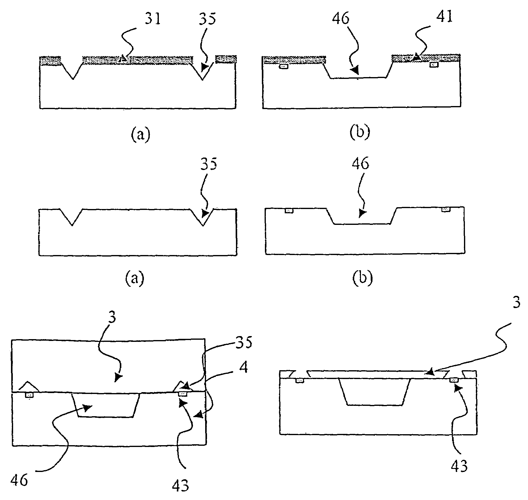
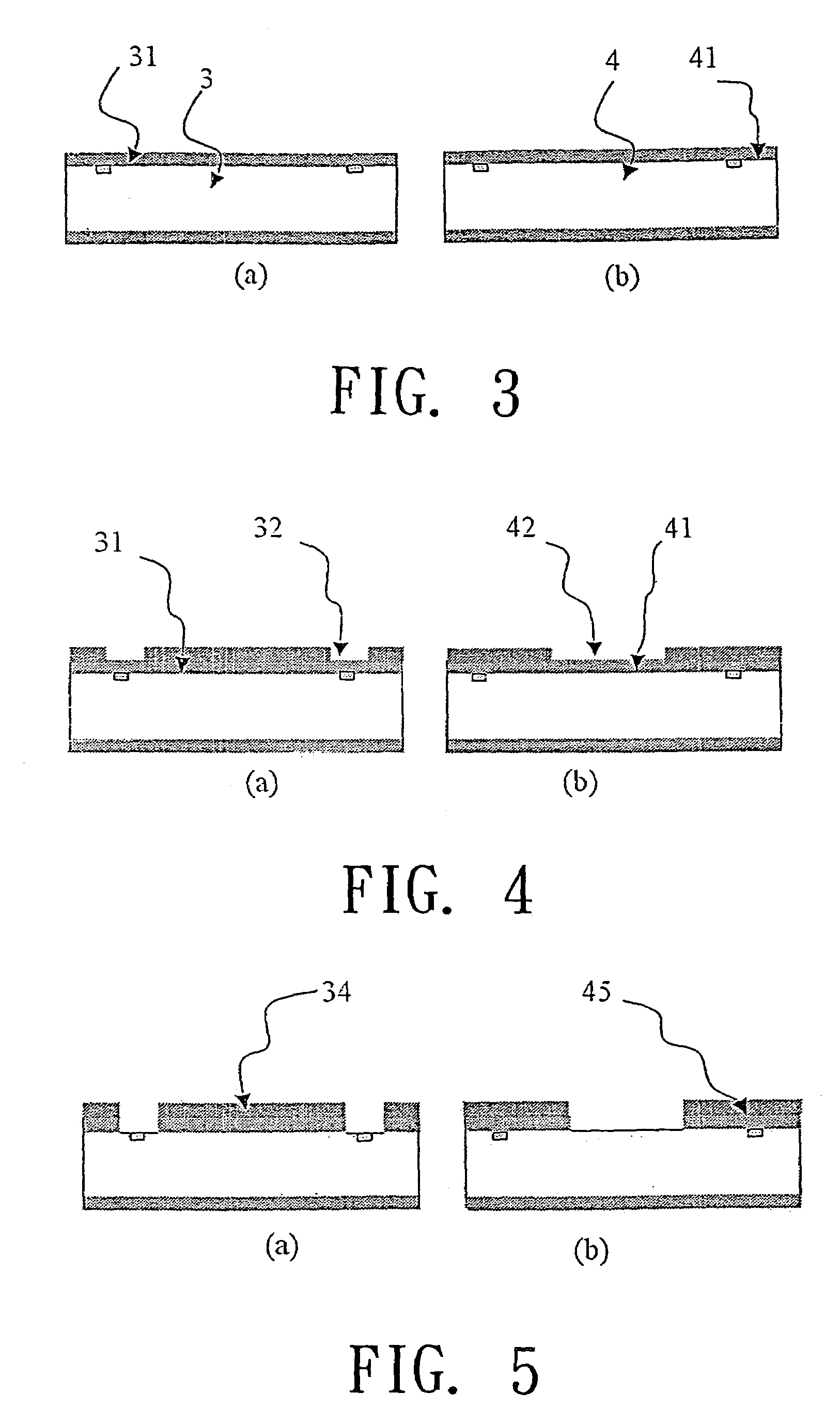
[0029]Now, by taking a pressure sensor for example, a n-type silicon wafer is used as a top wafer, while a p-type silicon wafer is used as a bottom wafer. A micro structure for the required cavity is formed on the bottom wafer. Two cavities are made by wet etching on the position corresponding to the alignment marks, and then the top and the bottom wafers are bonded by bonding the surface of the bottom wafer where the cavity is formed with the surface of the top wafer where the cavities are formed. The bonded wafer is then carried through the annealing treatment so as to ensure the bonding reliability. Finally the top wafer is thinned by grinding process to form a membrane with a desired thickness at the value ranging from several μm to ten times of several μm. The thickness of the membrane greatly affects the strength of output signal of a pressure sensor. As soon as the thickness of the membrane is reduced to less than the depth of the cavities formed on the bottom wafer, the alig...


PUM


Abstract

A method of maintaining photolithographic precision alignment for a wafer after being bonded, wherein two cavities are formed at the rear surface of a top wafer at the position corresponding to alignment marks made on a bottom wafer. The depth of both cavities is deeper than that of a final membrane structure. The top wafer is then bonded to the bottom wafer which already has alignment marks and a microstructure. This bonded wafer is annealed to intensify its bonding strength. After that, a thinning process is applied until the thickness of the top wafer is reduced to thinner than the cavity depth such that the alignment marks are emerged in the top wafer cavities thereby serving as alignment marks for any exposure equipment.

Description

BACKGROUND OF THE INVENTION[0001]1. Field of the Invention[0002]The present invention relates to a method of maintaining photolithographic precision alignment for a wafer after it is bonded. The method is performed by etching two cavities on a top wafer at the position corresponding to an alignment marks made on a bottom wafer. Afterwards, the bonded top and bottom wafers are treated with high temperature annealing process and thinning process successively so as to form a membrane structured wafer until the alignment marks made on the bottom wafer is exposed thereby providing a means for aligning the circuit pattern formed on the membrane to the structure of the bottom wafer.[0003]2. Description of the Prior Art[0004]In a book issued by Petersen et. al. in 1988 “Silicon Fusion Bonding for Pressure Sensors.” The book introduced a method of applying the wafer bonding process to fabrication techniques for a pressure sensor. It disclosed that a new membrane structured wafer can be obtai...

Claims


Application Information

Patent Timeline
Patent Type & Authority Patents(United States)
IPC IPC(8): G02B7/02H01L21/76H01L21/70H01L21/18
CPCB81C3/002H01L23/544H01L21/187H01L2223/54453H01L2224/83894H01L2924/01322Y10S438/975Y10S438/928Y10S438/977H01L2223/54426
Inventor TSENG, CHUNG-YANGGONG, SHIH-CHINHUANG, REUY-SHINGLEE, TONG-ANCHAN, KUO-CHUNGWANG, HUNG-DAR
Owner ASIA PACIFIC MICROSYST
Why Eureka
Try Eureka